Step-up dc-dc controller, Applications information – Rainbow Electronics MAX1771 User Manual
Page 13
MAX1771
12V or Adjustable, High-Efficiency,
Low I
Q
, Step-Up DC-DC Controller
______________________________________________________________________________________
13
Applications Information
Low Input Voltage Operation
When using a power supply that decays with time
(such as a battery), the N-FET transistor will operate in
its linear region when the voltage at EXT approaches
the threshold voltage of the FET, dissipating excessive
power. Prolonged operation in this mode may damage
the FET. This effect is much more significant in non-
bootstrapped mode than in bootstrapped mode, since
bootstrapped mode typically provides much higher
V
GS
voltages. To avoid this condition, make sure V
EXT
is above the V
TH
of the FET, or use a voltage detector
(such as the MAX8211) to put the IC in shutdown mode
once the input supply voltage falls below a predeter-
mined minimum value. Excessive loads with low input
voltages can also cause this condition.
Starting Up Under Load
The Typical Operating Characteristics show the Start-
Up Voltage vs. Load Current graph for bootstrapped-
mode operation. This graph depends on the type
of power switch used. The MAX1771 is not designed to
start up under full load in bootstrapped mode with low
input voltages.
Layout Considerations
Due to high current levels and fast switching wave-
forms, which radiate noise, proper PC board layout is
essential. Protect sensitive analog grounds by using a
star ground configuration. Minimize ground noise by
connecting GND, the input bypass capacitor ground
lead, and the output filter capacitor ground lead to a
single point (star ground configuration). Also, minimize
lead lengths to reduce stray capacitance, trace resis-
tance, and radiated noise. Place input bypass capaci-
tor C2 as close as possible to V+ and GND.
Excessive noise at the V+ input may falsely trigger the
timing circuitry, resulting in short pulses at EXT. If this
occurs it will have a negligible effect on circuit efficien-
cy. If desired, place a 4.7µF directly across the V+ and
GND pins (in parallel with the 0.1µF C2 bypass capaci-
tor) to reduce the noise at V+.
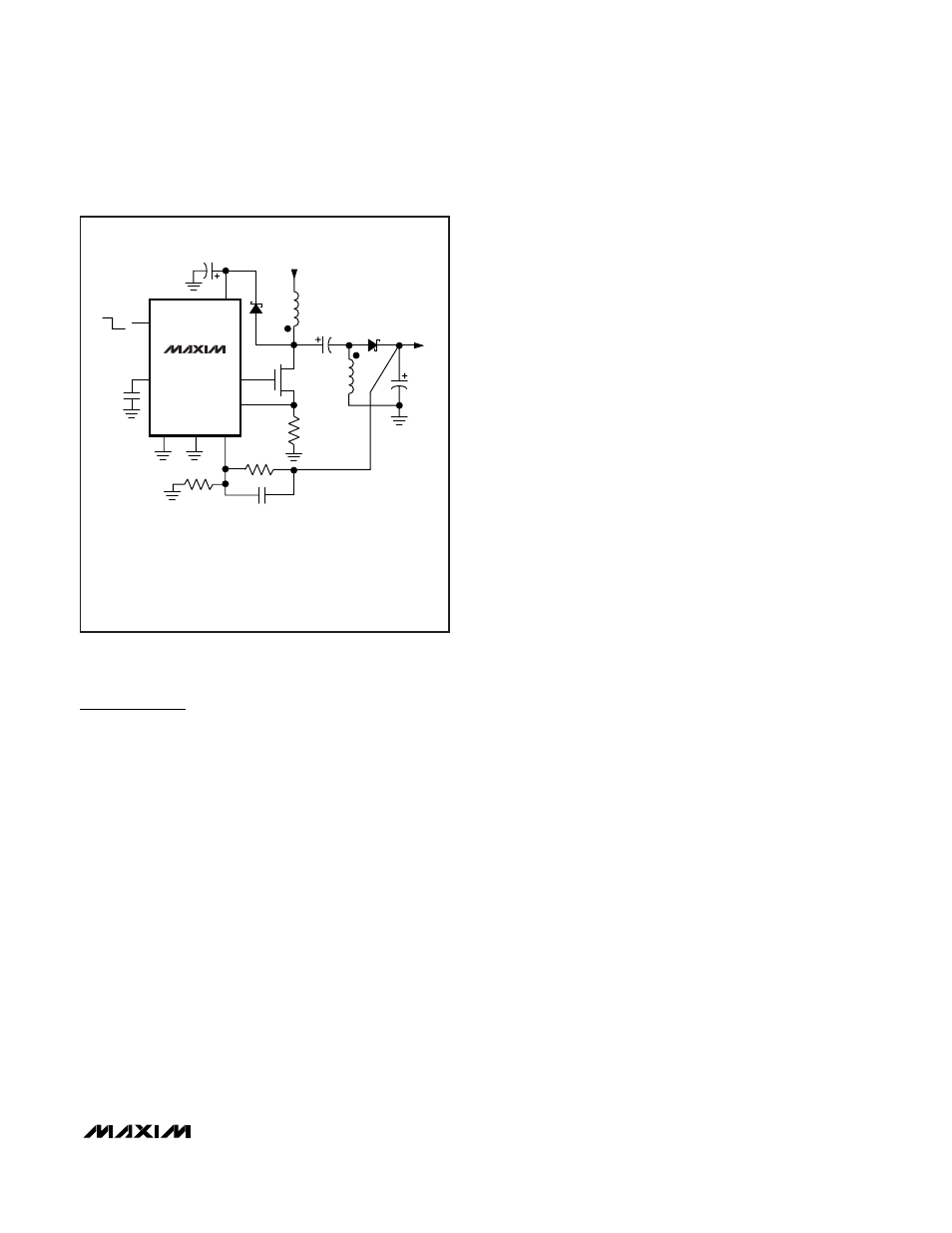
Other Application Circuits
4 Cells to 5V (or 3 Cells to 3.3V), 500mA
Step-Up/Down Converter
The circuit shown in Figure 5 generates 5V (or 3.3V) at
500mA with 85% efficiency, from an input voltage that
varies above and below the output. The output couples
to the switching circuitry via a capacitor. This configu-
ration offers two advantages over flyback-transformer
and step-up linear-regulator circuits: smooth regulation
as the input passes through the output, and no output
current in shutdown.
This circuit requires two inductors, which can be wound
on one core with no regard to coupling since they do
not work as a transformer. L1 and L2 can either be
wound together (as with the Coiltronics CTX20-4) or
kept as two separate inductors; both methods provide
equal performance. Capacitors C2 and C3 should be
low-ESR types for best efficiency. A 1µF ceramic
capacitor will work at C2, but with about 3% efficiency
loss. C2’s voltage rating must be greater than the maxi-
mum input voltage. Also note that the LX switch must
withstand a voltage equal to the sum of the input and
output voltage; for example, when converting 11V to
5V, the switch must withstand 16V.
LX switch pulses are captured by Schottky diode D2 to
boost V+ to (V
OUT
+ V
IN
). This improves efficiency with
a low input voltage, but also limits the maximum input
supply to 11V. If the input voltage does not fall below 4V
and if a 3V logic threshold FET is used for Q1, you may
omit D2 and connect V+ directly to the input supply.
12V Output Buck/Boost
The circuit in Figure 6 generates 12V from a 4.5V to
16V input. Higher input voltages are possible if you
MAX1771
SHDN
R1
0.1
Ω
REF
AGND
R2†
R3†
C5
47pF
GND
4
3V = OFF
5
FB
Q1**
SEE TEXT FOR FURTHER COMPONENT INFO
*
*
V
IN
MAY BE LOWER THAN INDICATED IF THE SUPPLY IS NOT
**
REQUIRED TO START UNDER FULL LOAD
**MOTOROLA MMFT3055ELT1
† FOR 5V: R2 = 200kΩ, R3 = 470kΩ
3.3V: R2 = 100k
Ω, R3 = 20kΩ
3
6
EXT
CS
1
L1
20
µH
1 CTX20-4
8
2
D2
1N5817
D1
1N5817
C3
220
µF
10V
C1
2.2
µF
C2
47
µF
16V
C4
0.1
µF
V+
V
IN
*
3V TO 11V
V
OUT
5V
500mA
7
L2
Figure 5. Step-Up/Down for a 5V/3.3V Output