Max3806 receiver for optical distance measurement, Pin configuration, Package information – Rainbow Electronics MAX3806 User Manual
Page 8: Table 2. output common-mode voltages

MAX3806
Receiver for Optical Distance Measurement
8
_______________________________________________________________________________________
made to either the GAIN or ATT setting. Table 2 pro-
vides typical output common-mode voltages for the
combination of settings. Settling time is proportional to
the RC time constant set by the output DC-blocking
capacitor, load, and MAX3806 output impedance. For
example, a 0.01µF DC-blocking capacitor, 2k
Ω load,
and 51
Ω output impedance provide an RC time con-
stant of approximately 20µs. After changing the GAIN
or ATT setting, the system should wait at least three to
four time constants before analyzing received signals.
Settling time is also required when changing the DIS
setting. When DIS is asserted high, the output disables
to high impedance and typically settles to steady state
within 200ns. When DIS is deasserted, the output
enables and typically settles to steady state within 50ns.
Overload Recovery Time
Transistors saturate when the amplifier is overloaded,
resulting in output distortion. Overload typically occurs
with signals greater than 20µA
P
(GAIN = 1) or 40µA
P
(GAIN = 0). It can withstand overload signals as large
as 2mA
P
. Recovery time depends on the amplitude and
duration of the overload pulse.
Layout Considerations
Noise performance and bandwidth are adversely affect-
ed by capacitance at the IN pad. Minimize capacitance
on this pad and select a low-capacitance photodiode.
Reducing PCB capacitance can be accomplished by
removing the ground plane underneath the connection
from the photodiode to the IN pin and by keeping the
photodiode as close as possible to the MAX3806.
Use broadband power-supply filtering techniques to
achieve the best sensitivity and noise performance.
Exposed-Pad Package and Thermal
Considerations
The exposed pad on the 12-pin TQFN provides a very
low thermal resistance path for heat removal from the IC.
The pad is also electrical ground on the MAX3806 and
must be soldered to the circuit board ground for proper
thermal and electrical performance. Refer to Application
Note 862:
HFAN-08.1: Thermal Considerations of QFN
and Other Exposed-Paddle Packages
for additional
information.
MAX3806
GND
GAIN
3
7
IN
N.C.
2
8
V
CC
OUT
1
9
12
4
V
CC
GND
11
5
N.C.
ATT
10
6
N.C.
DIS
THIN QFN
(3mm
×
3mm)
TOP VIEW
+
*EP
*EXPOSED PAD
V
CC
400
Ω
OUT
100
Ω
200
Ω
V
CC
Pin Configuration
PACKAGE TYPE
PACKAGE CODE
DOCUMENT NO.
12 TQFN-EP
T1233+1
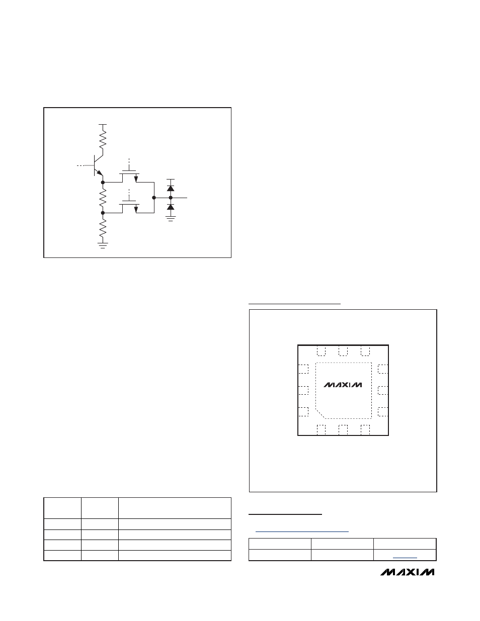
Figure 1. Equivalent Output Circuit
GAIN
ATT
OUTPUT COMMON-MODE
VOLTAGE (V)
0 0
1.65
0 1
0.33
1 0
1.82
1 1
0.36
Table 2. Output Common-Mode Voltages
Package Information
For the latest package outline information and land patterns, go
to
www.maxim-ic.com/packages
.
