0 dynamic performance, 0 common application pitfalls, Applications information – Rainbow Electronics ADC1175 User Manual
Page 17: Adc1 175
Applications Information
(Continued)
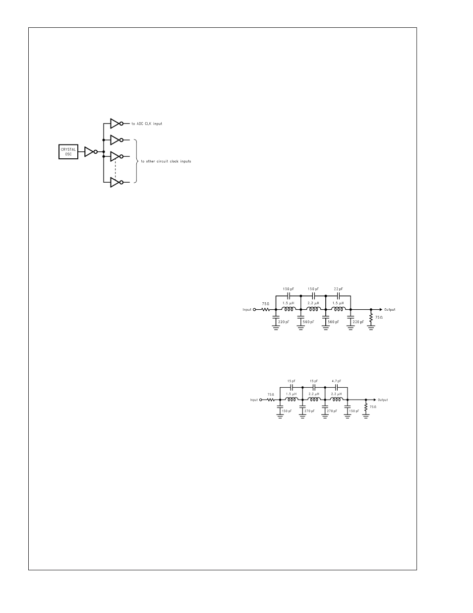
6.0 DYNAMIC PERFORMANCE
The ADC1175 is ac tested and its dynamic performance is
guaranteed. To meet the published specifications, the clock
source driving the CLK input must be free of jitter. For best
ac performance, isolating the ADC clock from any digital
circuitry should be done with adequate buffers, as with a
clock tree. See Figure 7.
It is good practice to keep the ADC clock line as short as
possible and to keep it well away from any other signals.
Other signals can introduce jitter into the clock signal.
7.0 COMMON APPLICATION PITFALLS
Driving the inputs (analog or digital) beyond the power
supply rails. For proper operation, all inputs should not go
more than 50mV below the ground pins or 50mV above the
supply pins. Exceeding these limits on even a transient basis
can cause faulty or erratic operation. It is not uncommon for
high speed digital circuits (e.g., 74F and 74AC devices) to
exhibit undershoot that goes more than a volt below ground.
A resistor of 50
Ω in series with the offending digital input will
usually eliminate the problem.
Care should be taken not to overdrive the inputs of the
ADC1175. Such practice may lead to conversion inaccura-
cies and even to device damage.
Attempting to drive a high capacitance digital data bus.
The more capacitance the output drivers must charge for
each conversion, the more instantaneous digital current is
required from DV
DD
and DGND. These large charging cur-
rent spikes can couple into the analog section, degrading
dynamic performance. Buffering the digital data outputs (with
an 74ACQ541, for example) may be necessary if the data
bus to be driven is heavily loaded. Dynamic performance
can also be improved by adding 47
Ω series resistors at each
digital output, reducing the energy coupled back into the
converter output pins.
Using an inadequate amplifier to drive the analog input.
As explained in Section 1.0, the capacitance seen at the
input alternates between 4 pF and 11 pF with the clock. This
dynamic capacitance is more difficult to drive than is a fixed
capacitance, and should be considered when choosing a
driving device. The CLC409, CLC440, LM6152, LM6154,
LM6181 and LM6182 have been found to be excellent de-
vices for driving the ADC1175 analog input.
Driving the V
RT
pin or the V
RB
pin with devices that can
not source or sink the current required by the ladder. As
mentioned in section 2.0, care should be taken to see that
any driving devices can source sufficient current into the V
RT
pin and sink sufficient current from the V
RB
pin. If these pins
are not driven with devices than can handle the required
current, these reference pins will not be stable, resulting in a
reduction of dynamic performance.
Using a clock source with excessive jitter, using an
excessively long clock signal trace, or having other
signals coupled to the clock signal trace. This will cause
the sampling interval to vary, causing excessive output noise
and a reduction in SNR performance. Simple gates with RC
timing is generally inadequate as a clock source.
Input test signal contains harmonic distortion that inter-
feres with the measurement of dynamic signal to noise
ratio. Harmonic and other interfering signals can be re-
moved by inserting a filter at the signal input. Suitable filters
are shown in Figure 8 and Figure 9. The circuit of Figure 8
has cutoff of about 5.5 MHz and is suitable for input frequen-
cies of 1 MHz to 5 MHz. The circuit of Figure 9 has a cutoff
of about 11 MHz and is suitable for input frequencies of 5
MHz to 10 MHz. These filters should be driven by a genera-
tor of 75 Ohm source impedance and terminated with a 75
ohm resistor.
10009217
FIGURE 7. Isolating the ADC clock from Digital
Circuitry.
10009218
FIGURE 8. 5.5 MHz Low Pass Filter to Eliminate
Harmonics at the Signal Input.
10009219
FIGURE 9. 11 MHz Low Pass filter to eliminate
harmonics at the signal input. Use at input frequencies
of 5 MHz to 10 MHz
ADC1
175
www.national.com
17