Specification definitions, Typical performance characteristics, Adc1 175 – Rainbow Electronics ADC1175 User Manual
Page 10

Typical Performance Characteristics
(Continued)
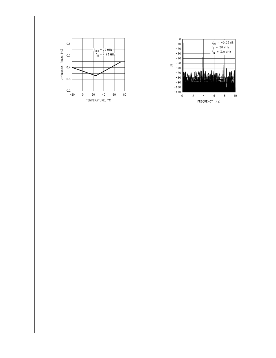
Differential Phase vs Temperature
Spectral Response at f
CLK
= 20 MSPS
10009227
10009228
Specification Definitions
ANALOG INPUT BANDWIDTH is a measure of the fre-
quency at which the reconstructed output fundamental drops
3 dB below its low frequency value for a full scale input. The
test is performed with f
IN
equal to 100 kHz plus integer
multiples of f
CLK
. The input frequency at which the output is
−3 dB relative to the low frequency input signal is the full
power bandwidth.
APERTURE JITTER is the time uncertainty of the sampling
point (t
DS
), or the range of variation in the sampling delay.
BOTTOM OFFSET is the difference between the input volt-
age that just causes the output code to transition to the first
code and the negative reference voltage. Bottom offset is
defined as E
OB
= V
ZT
- V
RB
, where V
ZT
is the first code
transition input voltage. Note that this is different from the
normal Zero Scale Error.
DIFFERENTIAL GAIN ERROR is the percentage difference
between the output amplitudes of a high frequency recon-
structed sine wave at two different dc levels.
DIFFERENTIAL NON-LINEARITY (DNL) is the measure of
the maximum deviation from the ideal step size of 1 LSB.
DIFFERENTIAL PHASE ERROR is the difference in the
output phase of a reconstructed small signal sine wave at
two different dc levels.
EFFECTIVE NUMBER OF BITS (ENOB, or EFFECTIVE
BITS) is another method of specifying Signal-to-Noise and
Distortion Ratio, or SINAD. ENOB is defined as (SINAD -
1.76) / 6.02 and says that the converter is equivalent to a
perfect ADC of this (ENOB) number of bits.
INTEGRAL NON-LINEARITY (INL) is a measure of the
deviation of each individual code from a line drawn from zero
scale (
1
⁄
2
LSB below the first code transition) through positive
full scale (
1
⁄
2
LSB above the last code transition). The devia-
tion of any given code from this straight line is measured
from the center of that code value. The end point test method
is used.
OUTPUT DELAY is the time delay after the rising edge of
the input clock before the data update is present at the
output pins.
OUTPUT HOLD TIME is the length of time that the output
data is valid after the rise of the input clock.
PIPELINE DELAY (LATENCY) is the number of clock cycles
between initiation of conversion and when that data is pre-
sented to the output stage. Data for any give sample is
available the Pipeline Delay plus the Output Delay after that
sample is taken. New data is available at every clock cycle,
but the data lags the conversion by the pipeline delay.
SAMPLING (APERTURE) DELAY is that time required after
the fall of the clock input for the sampling switch to open. The
Sample/Hold circuit effectively stops capturing the input sig-
nal and goes into the "hold" mode t
DS
after the clock goes
low.
SIGNAL TO NOISE RATIO (SNR) is the ratio of the rms
value of the input signal to the rms value of the other spectral
components below one-half the sampling frequency, not in-
cluding harmonics or dc.
SIGNAL TO NOISE PLUS DISTORTION (S/(N+D) or SI-
NAD) is the ratio of the rms value of the input signal to the
rms value of all of the other spectral components below half
the clock frequency, including harmonics but excluding dc.
SPURIOUS FREE DYNAMIC RANGE (SFDR) is the differ-
ence, expressed in dB, between the rms values of the input
signal and the peak spurious signal, where a spurious signal
is any signal present in the output spectrum that is not
present at the input.
TOP OFFSET is the difference between the positive refer-
ence voltage and the input voltage that just causes the
output code to transition to full scale and is defined as E
OT
=
V
FT
− V
RT
. Where V
FT
is the full scale transition input volt-
age. Note that this is different from the normal Full Scale
Error.
TOTAL HARMONIC DISTORTION (THD) is the ratio of the
rms total of the first six harmonic components, to the rms
value of the input signal.
ADC1
175
www.national.com
10
