0 the adc1175 clock, 0 layout and grounding, Applications information – Rainbow Electronics ADC1175 User Manual
Page 16

Applications Information
(Continued)
As is the case with all high speed converters, the ADC1175
should be assumed to have little power supply rejection,
especially when self-biasing is used by connecting V
RT
and
V
RTS
together.
No pin should ever have a voltage on it that is in excess of
the supply voltages or below ground, not even on a transient
basis. This can be a problem upon application of power to a
circuit. Be sure that the supplies to circuits driving the CLK,
OE, analog input and reference pins do not come up any
faster than does the voltage at the ADC1175 power pins.
4.0 THE ADC1175 CLOCK
Although the ADC1175 is tested and its performance is
guaranteed with a 20MHz clock, it typically will function with
clock frequencies from 1MHz to 30MHz.
If continuous conversions are not required, power consump-
tion can be reduced somewhat by stopping the clock at a
logic low when the ADC1175 is not being used. This reduces
the current drain in the ADC1175’s digital circuitry from a
typical value of 2.5mA to about 100µA.
Note that powering up the ADC1175 with the clock stopped
may not save power, as it will result in an increased current
flow (by as much as 170%) in the reference ladder. In some
cases, this may increase the ladder current above the speci-
fied limit. Toggling the clock twice at 1MHz or higher and
returning it to the low state will eliminate the excess ladder
current.
An alternative power-saving technique is to power up the
ADC1175 with the clock active, then halt the clock in the low
state after two clock cycles. Stopping the clock in the high
state is not recommended as a power-saving technique.
5.0 LAYOUT AND GROUNDING
Proper grounding and proper routing of all signals is essen-
tial to ensure accurate conversion. Separate analog and
digital ground planes that are connected beneath the
ADC1175 are required to meet data sheet limits. The analog
and digital grounds may be in the same layer, but should be
separated from each other. The analog and digital ground
planes should never overlap each other.
Capacitive coupling between the typically noisy digital
ground plane and the sensitive analog circuitry can lead to
poor performance that may seem impossible to isolate and
remedy. The solution is to keep the analog circuity well
separated from the digital circuitry and from the digital
ground plane.
Digital circuits create substantial supply and ground tran-
sients. The logic noise thus generated could have significant
impact upon system noise performance. The best logic fam-
ily to use in systems with A/D converters is one which
employs non-saturating transistor designs, or has low noise
characteristics, such as the 74HC(T) and 74AC(T)Q families.
Worst noise generators are logic families that draw the larg-
est supply current transients during clock or signal edges,
like the 74F and the 74AC(T) families. In general, slower
logic families, such as 74LS and 74HC(T), will produce less
high frequency noise than do high speed logic families, such
as the 74F and 74AC(T) families.
Since digital switching transients are composed largely of
high frequency components, total ground plane copper
weight will have little effect upon the logic-generated noise.
This is because of the skin effect. Total surface area is more
important than is total ground plane volume.
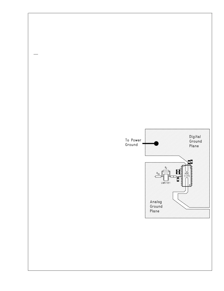
An effective way to control ground noise is by connecting the
analog and digital ground planes together beneath the ADC
with a copper trace that is very narrow (about 3/16 inch)
compared with the rest of the ground plane. This narrowing
beneath the converter provides a fairly high impedance to
the high frequency components of the digital switching cur-
rents, directing them away from the analog pins. The rela-
tively lower frequency analog ground currents do not see a
significant impedance across this narrow ground connection.
Generally, analog and digital lines should cross each other at
90 degrees to avoid getting digital noise into the analog path.
In video (high frequency) systems, however, avoid crossing
analog and digital lines altogether. Clock lines should be
isolated from ALL other lines, analog and digital. Even the
generally accepted 90 degree crossing should be avoided as
even a little coupling can cause problems at high frequen-
cies. Best performance at high frequencies and at high
resolution is obtained with a straight signal path.
Be especially careful with the layout of inductors. Mutual
inductance can change the characteristics of the circuit in
which they are used. Inductors should not be placed side by
side, not even with just a small part of their bodies being
beside each other.
The analog input should be isolated from noisy signal traces
to avoid coupling of spurious signals into the input. Any
external component (e.g., a filter capacitor) connected be-
tween the converter’s input and ground should be connected
to a very clean point in the analog ground return.
Figure 6 gives an example of a suitable layout. All analog
circuitry (input amplifiers, filters, reference components, etc.)
should be placed on or over the analog ground plane. All
digital circuitry and I/O lines should be placed over the digital
ground plane.
10009216
FIGURE 6. Layout example showing separate analog
and digital ground planes connected below the
ADC1175.
ADC1
175
www.national.com
16
