Rainbow Electronics DS1302 User Manual
Page 4
DS1302
041697 4/12
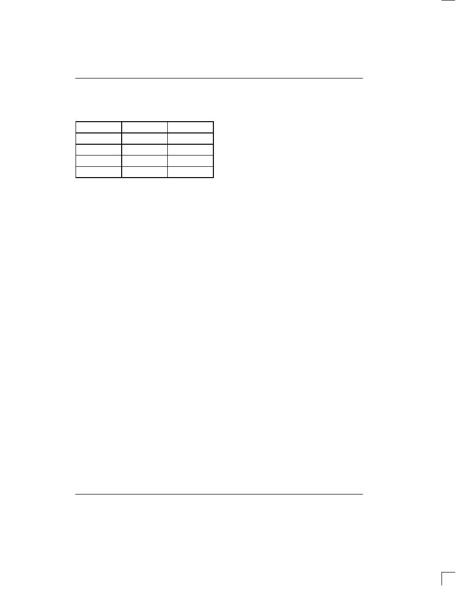
TCS. The RS bits (bits 0 – 1) select the resistor that is
connected between V
CC2
and V
CC1
. The resistor
selected by the resistor select (RS) bits is as follows:
RS Bits
Resistor
Typical Value
00
None
None
01
R1
2K
Ω
10
R2
4K
Ω
11
R3
8K
Ω
If RS is 00, the trickle charger is disabled independent
of TCS.
Diode and resistor selection is determined by the user
according to the maximum current desired for battery or
super cap charging. The maximum charging current
can be calculated as illustrated in the following example.
Assume that a system power supply of 5V is applied to
V
CC2
and a super cap is connected to V
CC1
. Also
assume that the trickle charger has been enabled with 1
diode and resistor R1 between V
CC2
and V
CC1
. The
maximum current I
max
would therefore be calculated as
follows:
I
max
= (5.0V – diode drop) / R1
~ (5.0V – 0.7V) / 2K
Ω
~ 2.2 mA
Obviously, as the super cap charges, the voltage drop
between V
CC2
and V
CC1
will decrease and therefore the
charge current will decrease.
CLOCK/CALENDAR BURST MODE
The clock/calendar command byte specifies burst
mode operation. In this mode the first eight clock/calen-
dar registers can be consecutively read or written (see
Figure 4) starting with bit 0 of address 0.
If the write protect bit is set high when a write clock/cal-
endar burst mode is specified, no data transfer will occur
to any of the eight clock/calendar registers (this includes
the control register). The trickle charger is not accessi-
ble in burst mode.
RAM
The static RAM is 31 x 8 bytes addressed consecutively
in the RAM address space.
RAM BURST MODE
The RAM command byte specifies burst mode opera-
tion. In this mode, the 31 RAM registers can be consec-
utively read or written (see Figure 4) starting with bit 0 of
address 0.
REGISTER SUMMARY
A register data format summary is shown in Figure 4.
CRYSTAL SELECTION
A 32.768 kHz crystal can be directly connected to the
DS1302 via pins 2 and 3 (X1, X2). The crystal selected
for use should have a specified load capacitance (CL) of
6 pF.
POWER CONTROL
V
CC1
provides low power operation in single supply and
battery operated systems as well as low power battery
backup.
V
CC2
provides the primary power in dual supply sys-
tems where V
CC1
is connected to a backup source to
maintain the time and data in the absence of primary
power.
The DS1302 will operate from the larger of V
CC1
or
V
CC2
. When V
CC2
is greater than V
CC1
+ 0.2V, V
CC2
will
power the DS1302. When V
CC2
is less than V
CC1
, V
CC1
will power the DS1302.