Rainbow Electronics DS1302 User Manual
Page 11
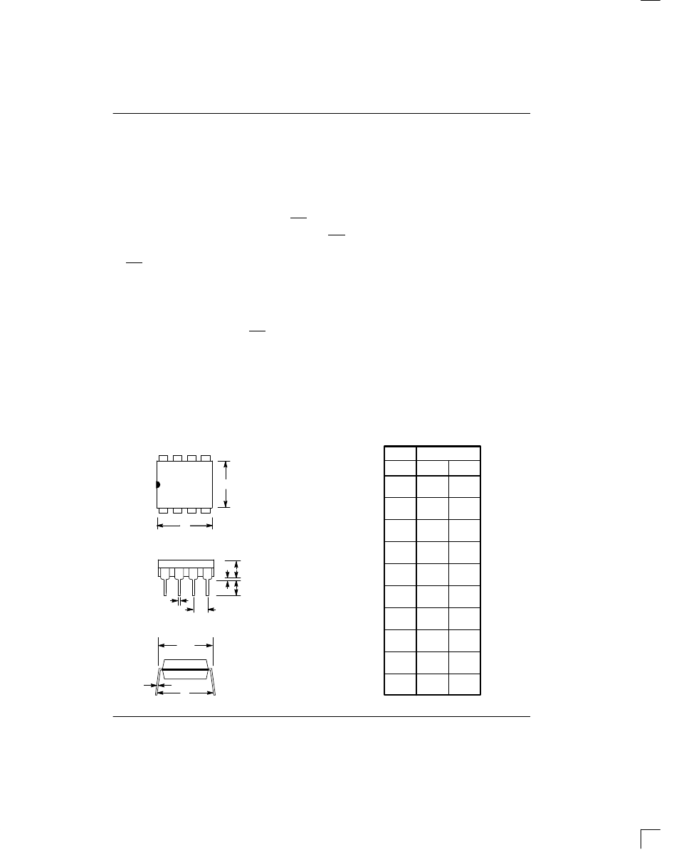
DIM
MIN
MAX
8–PIN
PKG
A IN.
MM
B IN.
MM
C IN.
MM
D IN.
MM
E IN.
MM
F IN.
MM
G IN.
MM
H IN.
MM
J IN.
MM
K IN.
MM
0.360
9.14
0.400
10.16
0.240
6.10
0.260
6.60
0.120
3.05
0.140
3.56
0.300
7.62
0.325
8.26
0.015
0.38
0.040
1.02
0.120
3.04
0.140
3.56
0.090
2.29
0.110
2.79
0.320
8.13
0.370
9.40
0.008
0.20
0.012
0.30
0.015
0.38
0.021
0.53
B
C
E
F
G
H
J
K
D
1
4
8
5
A
DS1302
041697 11/12
NOTES:
1. All voltages are referenced to ground.
2. Logic one voltages are specified at a source current of 1 mA at V
CC
=5V and 0.4 mA at V
CC
=2.5V, V
OH
=V
CC
for
capacitive loads.
3. Logic zero voltages are specified at a sink current of 4 mA at V
CC
=5V and 1.5 mA at V
CC
=2.5V, V
OL
=GND for
capacitive loads.
4. I
CC1T
and I
CC2T
are specified with I/O open, RST set to a logic “0”, and clock halt flag=0 (oscillator enabled).
5. I
CC1A
and I
CC2A
are specified with the I/O pin open, RST high, SCLK=2 MHz at V
CC
=5V; SCLK=500 kHz,
V
CC
=2.5V and clock halt flag=0 (oscillator enabled).
6. RST, SCLK, and I/O all have 40K
Ω
pulldown resistors to ground.
7. Measured at V
IH
=2.0V or V
IL
=0.8V and 10 ms maximum rise and fall time.
8. Measured at V
OH
=2.4V or V
OL
=0.4V.
9. Load capacitance = 50 pF.
10. I
CC1S
and I
CC2S
are specified with RST, I/O, and SCLK open. The clock halt flag must be set to logic one (oscillator
disabled).
11. V
CC
=V
CC2
, when V
CC2
>V
CC1
+0.2V; V
CC
=V
CC1
, when V
CC1
>V
CC2
.
12. V
CC2
=0 volts.
13. V
CC1
=0 volts.
14. Typical values are at 25
°
C.
DS1302 SERIAL TIMEKEEPER 8–PIN DIP