Operation, Command byte, Address/command byte figure 2 – Rainbow Electronics DS1302 User Manual
Page 2
1
7
6
A4
5
A3
4
A2
3
A1
2
A0
1
RD
0
W
RAM
CK
DS1302
041697 2/12
The DS1302 is the successor to the DS1202. In addi-
tion to the basic timekeeping functions of the DS1202,
the DS1302 has the additional features of dual power
pins for primary and back–up power supplies, program-
mable trickle charger for V
CC1
, and seven additional
bytes of scratchpad memory.
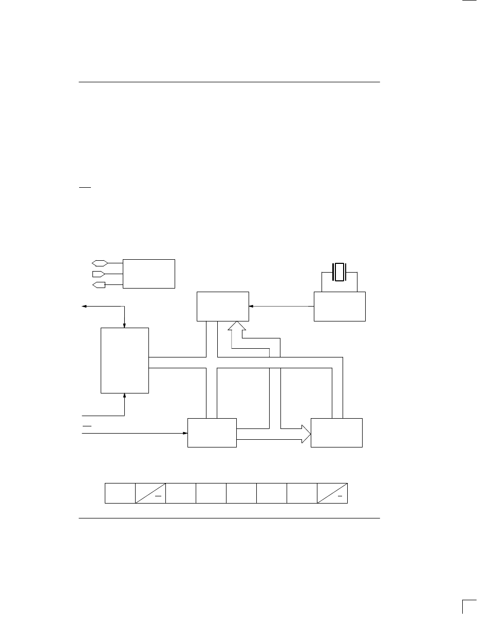
OPERATION
The main elements of the Serial Timekeeper are shown
in Figure 1: shift register, control logic, oscillator, real
time clock, and RAM. To initiate any transfer of data,
RST is taken high and eight bits are loaded into the shift
register providing both address and command informa-
tion. Data is serially input on the rising edge of the SCLK.
The first eight bits specify which of 40 bytes will be
accessed, whether a read or write cycle will take place,
and whether a byte or burst mode transfer is to occur.
After the first eight clock cycles have loaded the com-
mand word into the shift register, additional clocks will
output data for a read or input data for a write. The num-
ber of clock pulses equals eight plus eight for byte mode
or eight plus up to 248 for burst mode.
COMMAND BYTE
The command byte is shown in Figure 2. Each data
transfer is initiated by a command byte. The MSB (Bit 7)
must be a logic “1”. If it is zero, writes to the DS1302 will
be disabled. Bit 6 specifies clock/calendar data if logic
“0” or RAM data if logic “1”. Bits one through five specify
the designated registers to be input or output, and the
LSB (Bit 0) specifies a write operation (input) if logic “0”
or read operation (output) if logic “1”. The command
byte is always input starting with the LSB (Bit 0).
DS1302 BLOCK DIAGRAM Figure 1
32.768 kHz
X2
X1
OSCILLATOR
AND DIVIDER
REAL TIME
CLOCK
DATA BUS
INPUT SHIFT
REGISTERS
COMMAND AND
CONTROL LOGIC
ADDRESS BUS
31 X 8 RAM
I/O
SCLK
RST
POWER
CONTROL
V
CC1
V
CC2
GND
ADDRESS/COMMAND BYTE Figure 2