Ac electrical characteristics (continued) – Rainbow Electronics DS1124 User Manual
Page 3
DS1124
5.0V 8-Bit Programmable
Timing Element
_______________________________________________________________________________________
3
Note 1: All voltages are referenced to ground.
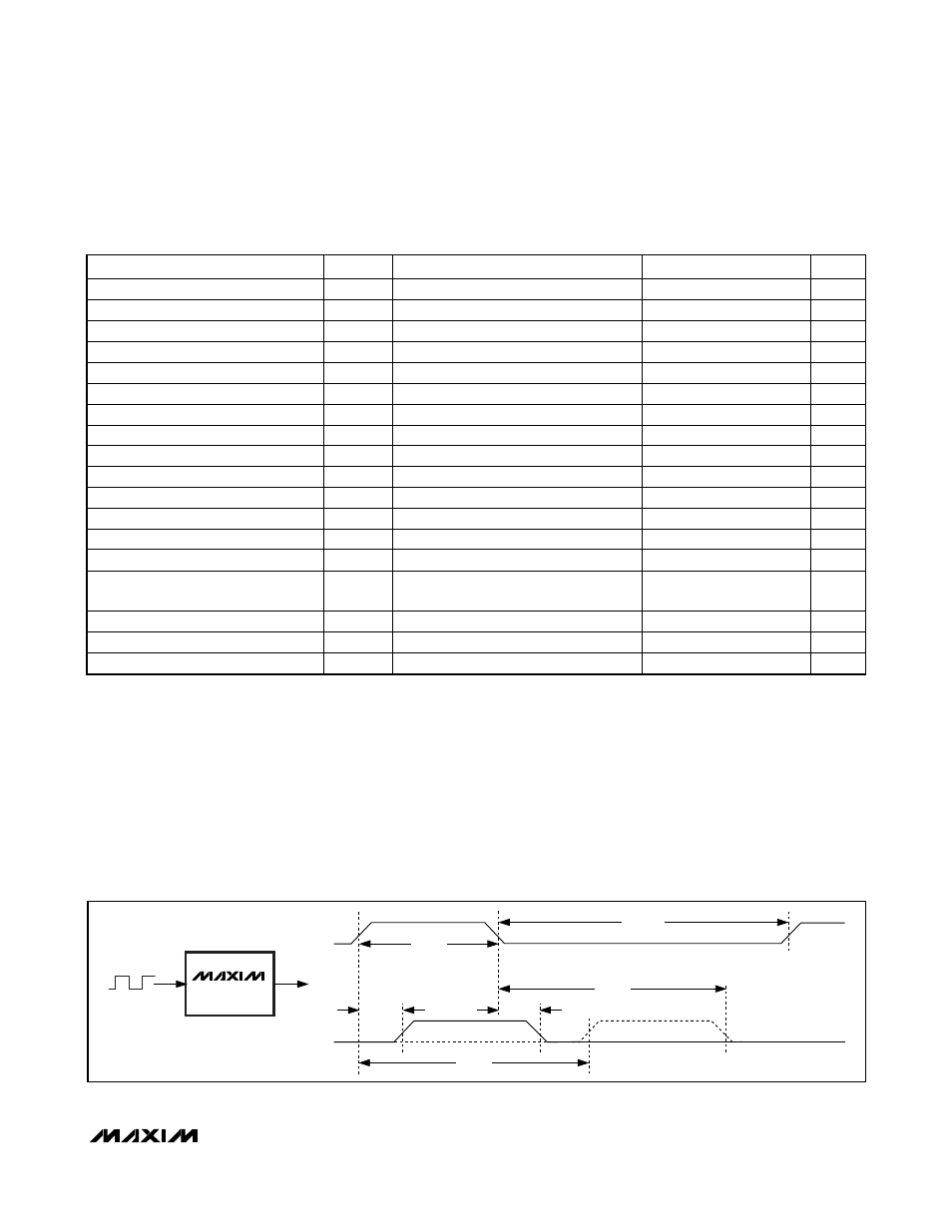
Note 2: Measured from rising edge of the input to the rising edge of the output. The programmed delay, t
D
, can be programmed
with values from 0 to 255. See Figure 1.
Note 3: See the
Integral Nonlinearity section and Figure 6.
Note 4: This is the minimum allowable interval between transitions on the input to ensure accurate device operation. This parameter
can be violated but timing accuracy may be impaired and ultimately very narrow pulse widths will result in no output from
the device. See Figure 1.
Note 5: When a 50% duty cycle input clock is used, this defines the highest usable clock frequency. When asymmetrical clock
inputs are used, the maximum usable clock frequency must be reduced to conform to the minimum input pulse-width
requirement. See Figure 1.
Note 6: Faster rise and fall times give the greatest accuracy in measured delay. Slow edges (outside the specification maximum)
can result in erratic operations.
AC ELECTRICAL CHARACTERISTICS (continued)
(V
CC
= +4.75V to +5.25V, T
A
= -40°C to +85°C, unless otherwise noted.)
PARAMETER
SYMBOL
CONDITIONS
MIN
TYP
MAX
UNITS
E to Delay Valid
t
EDV
50
μs
E to Delay Invalid
t
EDX
0
ns
Power-Up Time
t
PU
100 ms
Delay Step Size
t
STEP
T
A
= +25°C
-0.75
+0.25
+1
ns
Step 0 Delay
T
D0
(Note
2)
17 20 23 ns
Step 0 Delay Initial Accuracy
V
CC
= 5V, T
A
= +25°C
-0.6
+0.6
ns
Step 0 Voltage Variation
-0.4
+0.4
ns
Step 0 Temperature Variation
0°C to +70°C
-1
+1
ns
Step 0 Temperature Variation
-40°C to +85°C
-1
+1
ns
Step 255 Delay
T
D255
(Note
2)
77 83.75 88 ns
Step 255 Delay Initial Accuracy
V
CC
= 5V, T
A
= +25°C
-0.6
+0.6
ns
Step 255 Voltage Variation
-0.4
+0.4
ns
Step 255 Temperature Variation
0°C to +70°C
-3
+3
ns
Step 255 Temperature Variation
-40°C to +85°C
-5
+5
ns
Integral Nonlinearity
(Deviation from Straight Line)
t
ERR
T
A
= +25°C (Note 3)
-2
0
+2
ns
Minimum Input Pulse Width
t
WI
(Note
4)
40
ns
Minimum Input Period
t
PER
(Note
5)
80
ns
Input Rise and Fall Times
t
R
, t
F
(Note
6)
0 1
μs
t
D0
t
D0
t
D
t
WI
IN
OUT
t
WI
t
D
IN
TIMING REFERENCED TO 1.5V.
OUT
DS1124
Figure 1. Delay Timing Diagram