Dc electrical characteristics, Ac electrical characteristics – Rainbow Electronics DS1124 User Manual
Page 2
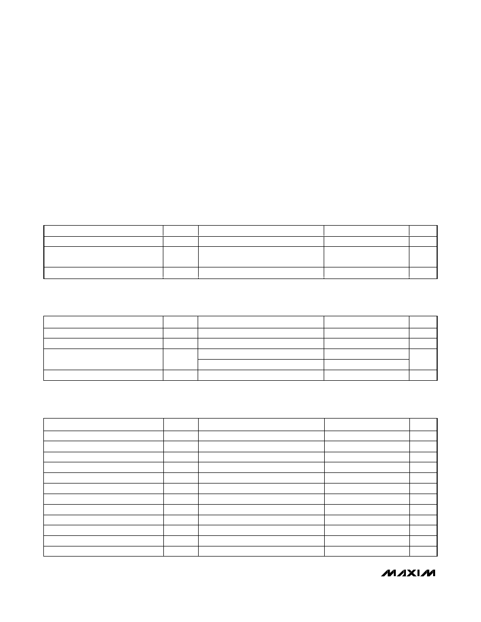
ABSOLUTE MAXIMUM RATINGS
RECOMMENDED OPERATING CONDITIONS
(TA = -40°C to +85°C)
Stresses beyond those listed under “Absolute Maximum Ratings” may cause permanent damage to the device. These are stress ratings only, and functional
operation of the device at these or any other conditions beyond those indicated in the operational sections of the specifications is not implied. Exposure to
absolute maximum rating conditions for extended periods may affect device reliability.
Voltage Range on V
CC
Pin Relative to Ground .....-0.5V to +6.0V
Voltage Range on IN, E, D, and CLK
Relative to Ground* ................................-0.5V to (V
CC
+ 0.5V)
Operating Temperature Range ...........................-40°C to +85°C
Storage Temperature Range .............................-55°C to +125°C
Short-Circuit Output Current ..........................50mA for 1 second
Soldering Temperature...................See J-STD-020 Specification
PARAMETER
SYMBOL
CONDITIONS
MIN
TYP
MAX
UNITS
Supply Voltage
V
CC
(Note 1)
4.75
5.25
V
Input Logic 1
V
IH
2.2
V
CC
+
0.3
V
Input Logic 0
V
IL
-0.3
+0.8
V
DC ELECTRICAL CHARACTERISTICS
(V
CC
= +4.75V to +5.25V, T
A
= -40°C to +85°C, unless otherwise noted.)
PARAMETER
SYMBOL
CONDITIONS
MIN
TYP
MAX
UNITS
Active Current
I
CCA
15
30
mA
High-Level Output Current
I
OH
V
CC
= min, V
OH
= 2.3V
-1.0
mA
Q pin, V
CC
= min, V
OL
= 0.5V
4.0
Low-Level Output Current
I
OL
OUT pin, V
CC
= min, V
OL
= 0.5V
8.0
mA
Input Leakage
I
L
-1.0 +1.0 μA
AC ELECTRICAL CHARACTERISTICS
(V
CC
= +4.75V to +5.25V, T
A
= -40°C to +85°C, unless otherwise noted.)
PARAMETER
SYMBOL
CONDITIONS
MIN
TYP
MAX
UNITS
Serial Clock Frequency
f
CLK
10 MHz
Input Pulse Width (E, CLK)
t
EW
, t
CW
50
ns
Data Setup to Clock
t
DSC
30
ns
Data Hold from Clock
t
DHC
0
ns
Data Setup to Enable
t
DSE
30
ns
Data Hold to Enable
t
DHE
0
ns
Enable Setup to Clock
t
ES
0
ns
Enable Hold from Clock
t
EH
30
ns
E to Q Valid
t
EQV
50
ns
E to Q High Impedance
t
EQZ
0
50
ns
CLK to Q Valid
t
CQV
50
ns
CLK to Q Invalid
t
CQX
0
ns
DS1124
5.0V 8-Bit Programmable
Timing Element
2
_______________________________________________________________________________________
*
Not to exceed +6.0V.