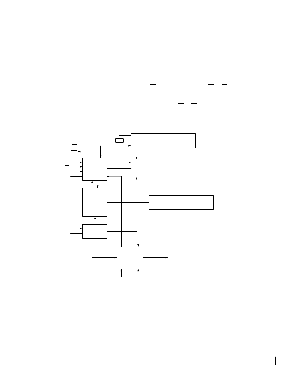
Operation, Timing block diagram figure 1 – Rainbow Electronics DS1215 User Manual
Page 2

DS1215
032697 2/15
OPERATION
The block diagram of Figure 1 illustrates the main ele-
ments of the Time Chip. Communication with the Time
Chip is established by pattern recognition of a serial bit
stream of 64 bits which must be matched by executing
64 consecutive write cycles containing the proper data
on data in (D). All accesses which occur prior to recog-
nition of the 64-bit pattern are directed to memory via the
chip enable output pin (CEO).
After recognition is established, the next 64 read or write
cycles either extract or update data in the Time Chip and
CEO remains high during this time, disabling the con-
nected memory.
Data transfer to and from the timekeeping function is ac-
complished with a serial bit stream under control of chip
enable input (CEI), output enable (OE), and write en-
able (WE). Initially, a read cycle using the CEI and OE
control of the Time Chip starts the pattern recognition
sequence by moving a pointer to the first bit of the 64 bit
comparison register. Next, 64 consecutive write cycles
are executed using the CEI and WE control of the Time
Chip. These 64 write cycles are used only to gain ac-
cess to the Time Chip.
TIMING BLOCK DIAGRAM Figure 1
CLOCK/CALENDAR LOGIC
UPDATE
TIMEKEEPING REGISTER
COMPARISON REGISTER
INTERNAL V
CC
V
CCO
V
CCI
X
1
X
2
D
Q
DATA
POWER-FAIL
WRITE
READ
CEO
ROM/RAM
BAT
1
BAT
2
32.768 kHz
CEI
OE
WE
RST
CONTROL
LOGIC
ACCESS
ENABLE
SEQUENCE
DETECTOR
I/O BUFFERS
POWER–FAIL
DETECT
LOGIC
