Rainbow Electronics DS1215 User Manual
Page 13

DS1215
032697 13/15
NOTES:
1. All voltages are referenced to ground.
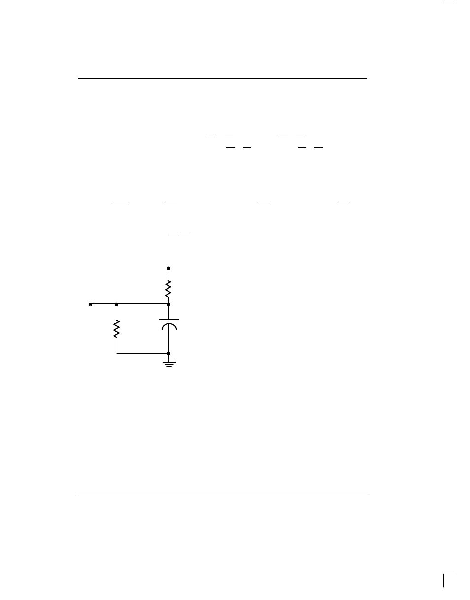
2. Measured with load shown in Figure 6.
3. Input pulse rise and fall times equal 10 ns.
4. t
WR
is a function of the latter occurring edge of WE or CE in RAM mode, or OE or CE in ROM mode.
5. t
DH
and t
DS
are functions of the first occurring edge of WE or CE in RAM mode, or OE or CE in ROM mode.
6. Measured without RAM connected.
7. Trip point voltage for power–fail detect. V
TP
= 1.26 x V
BAT
. For 10% V
CC
= 5V + 10% operation V
BAT
= 3.5V max.;
for 5% operation V
BAT
= 3.7V max.
8. I
CC01
is the maximum average load current the DS1215 can supply to memory.
9. Applies to CEO with the ROM/RAM pin grounded. When the ROM/RAM pin is connected to V
CCO
, CEO will go
to a low level as V
CCI
falls below V
BAT
.
10. I
CC02
is the maximum average load current that the DS1215 can supply to memory in the battery backup mode.
11. Applies to all input pins except RST. RST is pulled internally to V
CCI
.
OUTPUT LOAD Figure 6
+5V
50 pF
680
Ω
1.1K
Ω
- MAX6869 (17 pages)
- TNY-A9260-C01 (5 pages)
- MAX34441 (53 pages)
- MAX4912 (13 pages)
- QIL-A9260-C11 (34 pages)
- QIL-A9260-C11 (20 pages)
- QIL-A9260-C11 (1 page)
- USB-A9263-C02 (1 page)
- DAB-GPS-C01 (15 pages)
- DAB-GPS-C01 (28 pages)
- DAB-CAM-C01 (27 pages)
- DAB-WLS-C01 (WiFi) (20 pages)
- USB-A9G20-C01 (1 page)
- MAX34440 (43 pages)
- SBC35-A9260-C12 (28 pages)
- SBC35-A9260-C12 (1 page)
- MAX16024 (17 pages)
- USB-A9G20-C11 (5 pages)
- DAB-IMU-C01 (20 pages)
- MAX16021 (21 pages)
- DAB-WLS-C11 (BlueTooth) (2 pages)
- SBC35-A9G20-C11 (24 pages)
- MAX16054 (9 pages)
- MAX14525 (7 pages)
- MAX16066 (61 pages)
- USB-A9260-C12 (1 page)
- DS1803 (11 pages)
- DS12887A (2 pages)
- DS1339 (18 pages)
- DS1858 (22 pages)
- DS1267 (12 pages)
- DS12С887A (2 pages)
- DS1804 (7 pages)
- DS1091L (6 pages)
- DS1669S (10 pages)
- DS1867 (14 pages)
- DS1087L (12 pages)
- DS4026 (13 pages)
- DS1286 (13 pages)
- DS1801 (10 pages)
- DS1254 (17 pages)
- DS17887 (38 pages)
- DS1691 (4 pages)
- DS1615 (24 pages)
- DS1868 (14 pages)
