Atr0630, Atr0630 [preliminary, Pin configuration – Rainbow Electronics ATR0630 User Manual
Page 6: 1 pinout
6
4920A–GPS–01/06
ATR0630 [Preliminary]
3.
Pin Configuration
3.1
Pinout
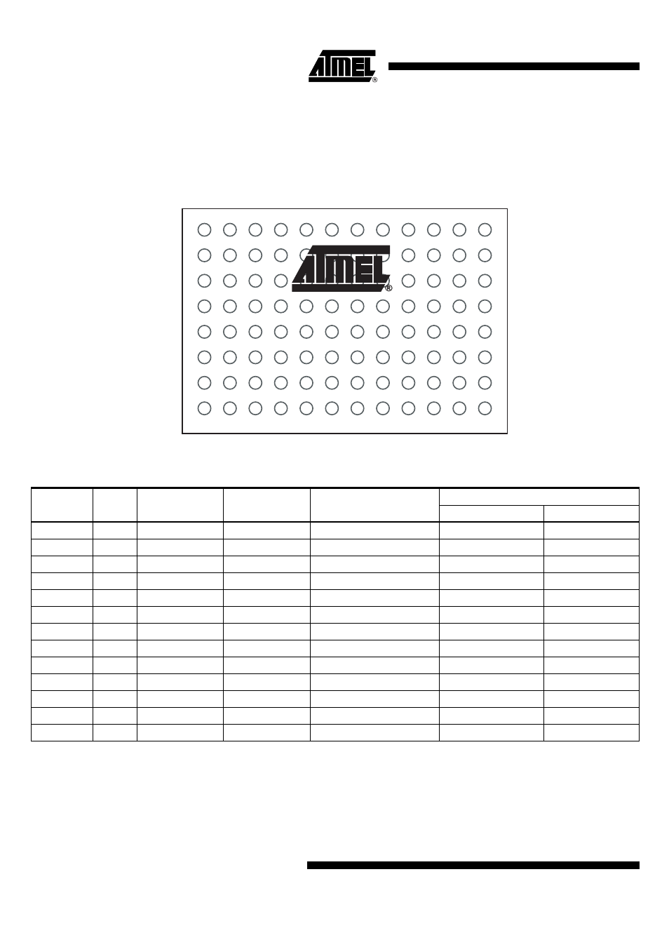
Figure 3-1.
Pinning BGA96 (Top View)
Table 3-1.
ATR0630 Pinout
Pin Name
BGA 96
Pin Type
Pull Resistor
(Reset Value)
(1)
Firmware Label
PIO Bank A
I
O
AGCO
A4
Analog I/O
CLK23
A8
Digital IN
DBG_EN
E8
Digital IN
PD
EGC
D4
Digital IN
GDIG
C5
Supply
GND
A6
Supply
GND
A9
Supply
GND
B11
Supply
GND
F5
Supply
GND
H8
Supply
GND
H12
Supply
GNDA
A3
Supply
GNDA
B1
Supply
Notes:
1. PD = internal pull-down resistor, PU = internal pull-up resistor, OH = switched to Output High at reset
2. VBAT18 represent the internal power supply of the backup power domain, see section
3. VDD_USB is the supply voltage for following the USB pins: USB_DM and USB_DP, see section
. For operation of the USB interface, supply of 3.0V to 3.6V is required.
4. VDDIO is the supply voltage for the following GPIO pins: P1, P2, P8, P12, P14, P16, P17, P18, P19, P20, P21, P23, P24,
P25, P26, P27 and P29, see section
.
A
B
C
D
E
F
G
H
1
2
3
4
5
6
7
8
9
10
11
12
ATR0630