Rainbow Electronics DS1670 User Manual
Page 4
DS1670
4 of 17
POWER-UP/POWER-DOWN CONSIDERATIONS
The DS1670 was designed to operate with a power supply of 3.3 volts. When 3.3 volts are applied within
nominal limits, the device becomes fully accessible after t
RPU
(250 ms typical). Before t
RPU
elapses, all
inputs are disabled. When V
CC
drops below 2.88 volts (typical), the
RST
pin is driven low. When V
CC
drops below the lower of 2.7 volts (typical) or the battery voltage, the device is switched over to the
backup power supply.
During power up, when V
CC
returns to an in-tolerance condition, the
RST
pin is kept in the active state
for 250 ms (typical) to allow the power supply and microprocessor to stabilize.
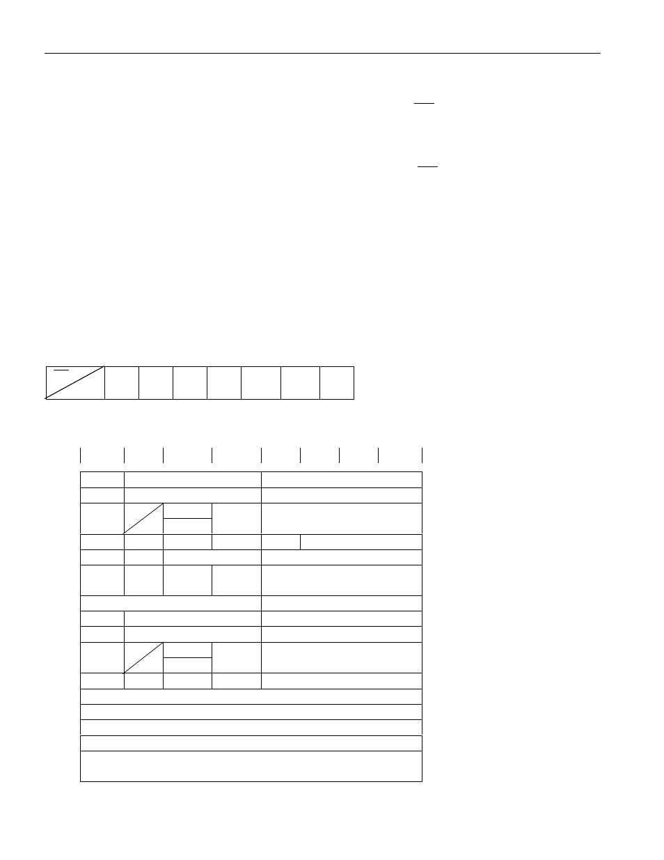
ADDRESS/COMMAND BYTE
The command byte for the DS1670 is shown in Figure 2. Each data transfer is initiated by a command
byte. Bits 0 through 6 specify the addresses of the registers to be accessed. The MSB (bit 7) is the
Read/Write bit. This bit specifies whether the accessed byte will be read or written. A read operation is
selected if bit 7 is a 0 and a write operation is selected if bit 7 is a 1. The address map for the DS1670 is
shown in Figure 3.
ADDRESS/COMMAND BYTE Figure 2
7
6
5
4
3
2
1
0
RD
WR
A6
A5
A4
A3
A2
A1
A0
DS1670 ADDRESS MAP Figure 3
BIT 7
BIT 0
00
0
10 SECONDS
SECONDS
01
0
10 MINUTES
MINUTES
10 HR
02
0
12
24
A/P
10 HR
HOURS
03
0
0
0
0
0
DAY
04
0
0
10 DATE
DATE
05
0
0
0
10
MO.
MONTH
06
10 YEAR
YEAR
07
M
10 SEC ALARM
SECONDS ALARM
08
M
10 MIN ALARM
MINUTES ALARM
10 HR
09
M
12
24
A/P
10 HR
HOUR ALARM
0A
M
0
0
0
DAY ALARM
0B
CONTROL REGISTER
0C
STATUS REGISTER
0D
WATCHDOG REGISTER
0E
ADC REGISTER
0F
7F
RESERVED