Irfts9342pbf, Thermal resistance, Static @ t – Rainbow Electronics IRFTS9342TRPBF User Manual
Page 2: 25°c (unless otherwise specified), Diode characteristics
IRFTS9342PbF
2
www.irf.com
G
D
S
Notes:
Repetitive rating; pulse width limited by max. junction temperature.
Pulse width
≤ 400μs; duty cycle ≤ 2%.
When mounted on 1 inch square copper board.
Thermal Resistance
Parameter
Typ.
Max.
Units
R
θJA
Junction-to-Ambient
e
–––
62.5
°C/W
Static @ T
J
= 25°C (unless otherwise specified)
Parameter
Min. Typ. Max. Units
BV
DSS
Drain-to-Source Breakdown Voltage
-30
–––
–––
V
ΔΒV
DSS
/
ΔT
J
Breakdown Voltage Temp. Coefficient
–––
19
––– mV/°C
R
DS(on)
Static Drain-to-Source On-Resistance
–––
32
40
–––
53
66
V
GS(th)
Gate Threshold Voltage
-1.3
–––
-2.4
V
ΔV
GS(th)
Gate Threshold Voltage Coefficient
–––
-5.5
––– mV/°C
I
DSS
Drain-to-Source Leakage Current
–––
–––
-1.0
–––
–––
-150
I
GSS
Gate-to-Source Forward Leakage
–––
–––
-100
Gate-to-Source Reverse Leakage
–––
–––
100
gfs
Forward Transconductance
6.8
–––
–––
S
Q
g
Total Gate Charge
–––
12
–––
Q
gs
Gate-to-Source Charge
–––
1.8
–––
Q
gd
Gate-to-Drain Charge
–––
3.1
–––
R
G
Gate Resistance
–––
17
–––
Ω
t
d(on)
Turn-On Delay Time
–––
4.6
–––
t
r
Rise Time
–––
13
–––
t
d(off)
Turn-Off Delay Time
–––
45
–––
t
f
Fall Time
–––
28
–––
C
iss
Input Capacitance
–––
595
–––
C
oss
Output Capacitance
–––
133
–––
C
rss
Reverse Transfer Capacitance
–––
85
–––
Diode Characteristics
Parameter
Min. Typ. Max. Units
I
S
Continuous Source Current
(Body Diode)
I
SM
Pulsed Source Current
(Body Diode)
Ã
V
SD
Diode Forward Voltage
–––
–––
-1.2
V
t
rr
Reverse Recovery Time
–––
20
30
ns
Q
rr
Reverse Recovery Charge
–––
11
17
nC
t
on
Forward Turn-On Time
Time is dominated by parasitic Inductance
V
DS
= V
GS
, I
D
= -25μA
V
GS
= -4.5V, I
D
= -4.6A
e
m
Ω
V
DD
= -15V, V
GS
= -10V
V
DS
= -15V
R
G
= 6.8
Ω
V
DS
= -10V, I
D
= -4.6A
V
DS
= -24V, V
GS
= 0V, T
J
= 125°C
μA
I
D
= -4.6A
I
D
= -4.6A
V
GS
= 0V
V
DS
= -25V
V
DS
= -24V, V
GS
= 0V
T
J
= 25°C, I
F
= -4.6A, V
DD
= -24V
di/dt = 100A/μs
eÃ
T
J
= 25°C, I
S
= -4.6A, V
GS
= 0V
e
showing the
integral reverse
p-n junction diode.
Conditions
ƒ = 1.0KHz
Conditions
V
GS
= 0V, I
D
= -250μA
Reference to 25°C, I
D
= -1mA
V
GS
= -10V, I
D
= -5.8A
e
–––
–––
-46
–––
–––
-2.0
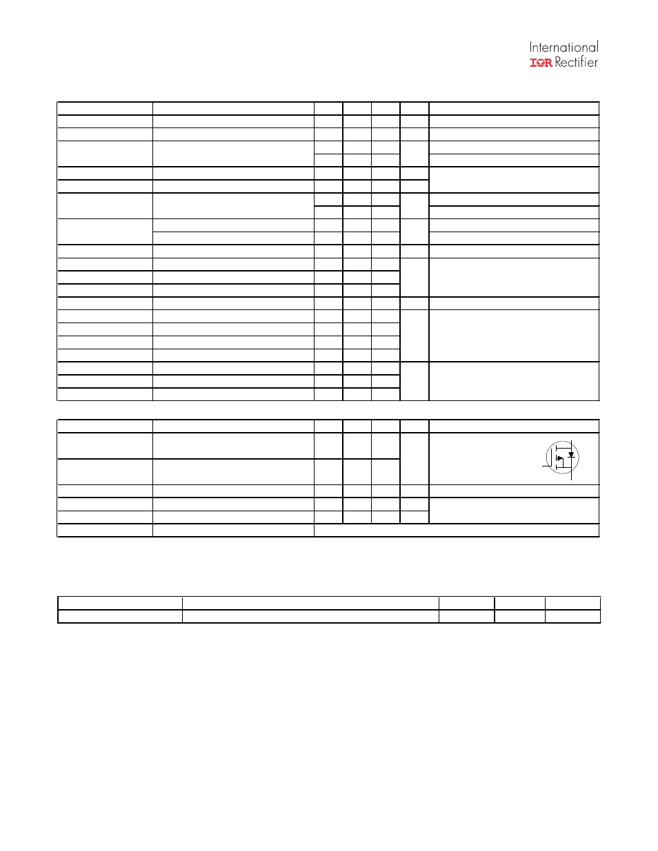
MOSFET symbol
nA
ns
A
pF
nC
V
GS
= -10V
V
GS
= -20V
V
GS
= 20V