Atr0600 [preliminary, Pin configuration, Pin description – Rainbow Electronics ATR0600 User Manual
Page 2
2
ATR0600 [Preliminary]
4536F–GPS–10/03
Pin Configuration
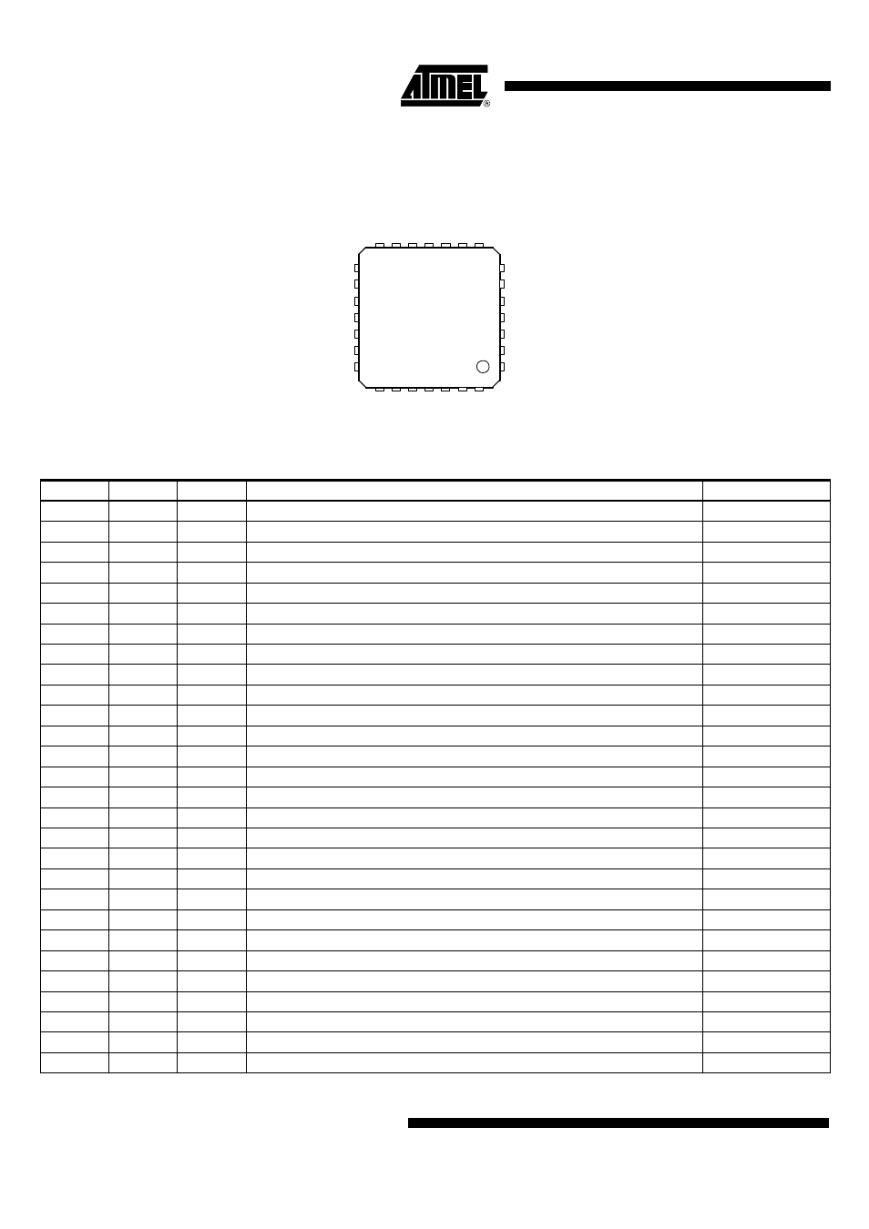
Figure 2. Pinning QFN28
BP
NBP
BPI
NBPI
VS1
n.c.
n.c.
X
VS5
XTO
NXTO
VS7
NX
AGCO
n.
c.
R
F
N
IN
R
F
IN
V
S
3
P
1
P
2
n.
c.
G
C
V
S
2
R
E
F
S
IG
L
S
IG
H
V
D
IG
S
C
14 13 12 11 10 9 8
22 23 24 25 26 27 28
15
16
17
18
19
20
21
7
6
5
4
3
2
1
Pin Description
Pin
Symbol
Type
Function
Protection Level
1
AGCO
O
Signal level output
ESD3
2
NX
OB
Complementary to X
ESD3
3
VS7
P
ECL - blocks supply
ESD2
4
NXTO
IB
Complementary to XTO
ESD3
5
XTO
IB
Quartz input
ESD3
6
VS5
P
XTO supply
ESD2
7
X
OB
Quartz intermediate output
ESD3
8
n.c.
–
Not connected
–
9
P2
I
Power-up quartz oscillator
ESD3
10
P1
I
Power-up RF part
ESD3
11
VS3
P
Reference supply
ESD2
12
RFIN
IB
RF input 1.575 GHz
ESD3
13
RFNIN
IB
Complementary to RFIN
ESD3
14
n.c.
–
Not connected
–
15
BP
IB
Open-collector output of mixer
ESD3
16
NBP
IB
Complementary to BP
ESD3
17
BPI
IB
IF - filter input
ESD3
18
NBPI
IB
Complementary to BPI
ESD3
19
VS1
P
VCO + mixer + VGA supply
ESD2
20
n.c.
–
Not connected
–
21
n.c.
–
Not connected
–
22
GC
I
Gain control input
ESD3
23
VS2
P
Subsampling unit supply
ESD2
24
REF
O
Defining low threshold voltage
ESD3
25
SIGL
O
Digital interface subsampled output high threshold voltage refered to REF1
ESD3
26
SIGH
O
Digital interface subsampled output low threshold voltage refered to REF2
ESD3
27
VDIG
P
Digital interface supply voltage 1.8 V
ESD2
28
SC
O
Digital interface clock output
ESD3