Through the v, Pin. the chip-enable output to sram, Pulse width of t – Rainbow Electronics DS1680 User Manual
Page 2
DS1680
2 of 23
Automatic backup and write protection of an external SRAM is provided through the V
CCO
and
CEO pins. The backup energy source used to power the RTC is also used to retain RAM data in the
absence of V
CC
through the V
CCO
pin. The chip-enable output to SRAM,
CE0
, is controlled during power
transients to prevent data corruption.
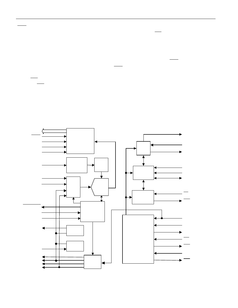
The DS1680’s microprocessor- monitor circuitry provides three basic functions. First, a precision
temperature-compensated reference and comparator circuit monitors the status of V
CC
. When an out-of-
tolerance condition occurs, an internal power-fail signal is generated that forces
RST to the active state.
When V
CC
returns to an in- tolerance condition, the
RST signal is kept in the active state for t
RPU
to allow
the power supply and processor to stabilize. The DS1680 debounces a pus hbutton input and guarantees an
active
RST
pulse width of t
RST
. The third function is a watchdog timer. The DS1680’s internal timer
forces the
RST
signal to the active state if the strobe input is not driven low prior to watchdog time-out.
The DS1680 also provides a touch-screen controller along with a 10-bit successive approximation ADC.
The ADC is monotonic (no missing codes) and has an internal analog filter to reduce high frequency
noise.
DS1680 BLOCK DIAGRAM Figure 1
CLOCK
OSC
CLOCK
GEN
PANEL
DRIVE
CONVERT
CONTROL
10-BIT
ADC
INPUT
MUX
TOUCH
DETECT
POWER
CONTROL
RTC
SERIAL
INTERFACE
WATCHDOG
OUTPUT
MUX
BHE
OUT_SELECT
PEN_SELECT
AIN0
AIN1
COEN
CONVERT
PEN_OFF
PD_RST
D0-D7
OSCIN
X1
X2
INT
SCLK
CS
I/O
ST
RST
POWER SWITCH,
WRITE PROTECT,
NV CONTROL,
AND
POWER FAIL
WARNING
V
CC
V
BAT
V
CCO
CEI
CEO
PFI
PFO
ANSELIN
X+
X-
Y+
Y-
NEW_DATA