Pin description – Rainbow Electronics DS2127 User Manual
Page 4
DS2127
Ultra3 LVD/SE SCSI 14-Line Terminator
4
_____________________________________________________________________
Pin Description
PIN
NAME
FUNCTION
1, 2, 11–24,
37–48
R_ _ P, R_ _ N
Signal Termination. Connect to SCSI bus signal lines. Asserting ISO removes the terminators from the
SCSI bus. R_ _ P pins are the ground line for SE operation and the positive lines in differential mode.
R_ _ N pins are the signal lines in SE operation and the negative lines in differential mode.
3
TPWR
Termination Power. Connect to the SCSI TERMPWR line and decouple with a ceramic
2.2µF capacitor.
4–9, 28–33
HS_GND
Heat-Sink Ground. Internally connected to the mounting pad. These pins must be connected to
ground. These pins should be connected to a ground plane with the layout optimized for
heat transfer.
10
V
REF
Regulator Output Voltage. This must be decoupled with a 4.7µF capacitor. Asserting ISO floats this
output. A high-frequency capacitor (0.1µF) should also be placed on the V
REF
pin in applications that
use fast rise/fall-time drivers.
25
GND
Signal Ground
26
SE
SE Mode Indicator. A high state indicates SE mode detected on SCSI bus.
27
LVD
LVD Mode Indicator. A high state indicates LVD mode detected on SCSI.
34
DIFF_CAP
DIFFSENSE Capacitor. Connect a 0.1µF capacitor for the DIFFSENSE filter. Input to detect the type of
device (differential or single-ended) on the SCSI bus.
35
DIFFSENS
DIFFSENSE. Output to drive the SCSI bus DIFFSENS line.
36
ISO
Isolation Input. When pulled high, terminating resistors and biasing current sources are removed from
the SCSI bus. When not connected to ground, the pin has a 10µA current source pulling the pin to the
high state.
2.15V
0.6V
THERMAL
SHUTDOWN
1.30V
DIFF_CAP
ISO
2.15V
1.30V
1.25V
(LVD)
R1N
R1P
R14N
R14P
V
REF
0.6V
DIFFSENS
2.85V
(SE)
LVD
SE
HVD
LVD SE HVD
LVD
SE
LVD
SE
CONTROL LOGIC
DELAY/
FILTER
BANDGAP
REFGEN AND
TRIM
10
µA
52
Ω
52
Ω
52
Ω
52
Ω
110
Ω
110
Ω
124
Ω
124
Ω
SE
ALL SWITCHES UP
HVD/ISO
ALL SWITCHES CENTER
LVD
ALL SWITCHES DOWN
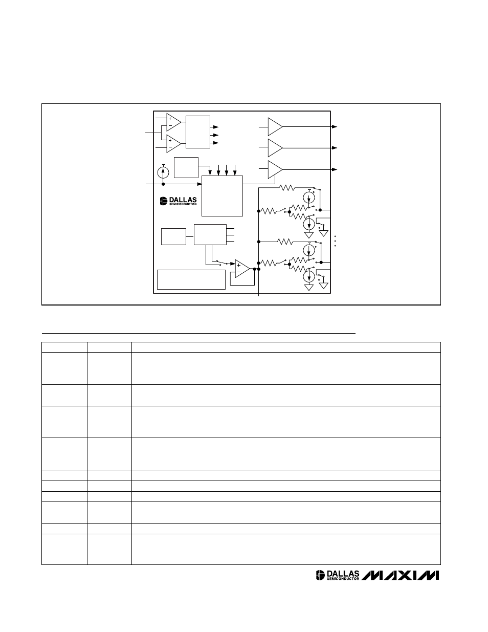
DS2127
Figure 1. Block Diagram