Converter electrical characteristics – Rainbow Electronics ADC10D020 User Manual
Page 9

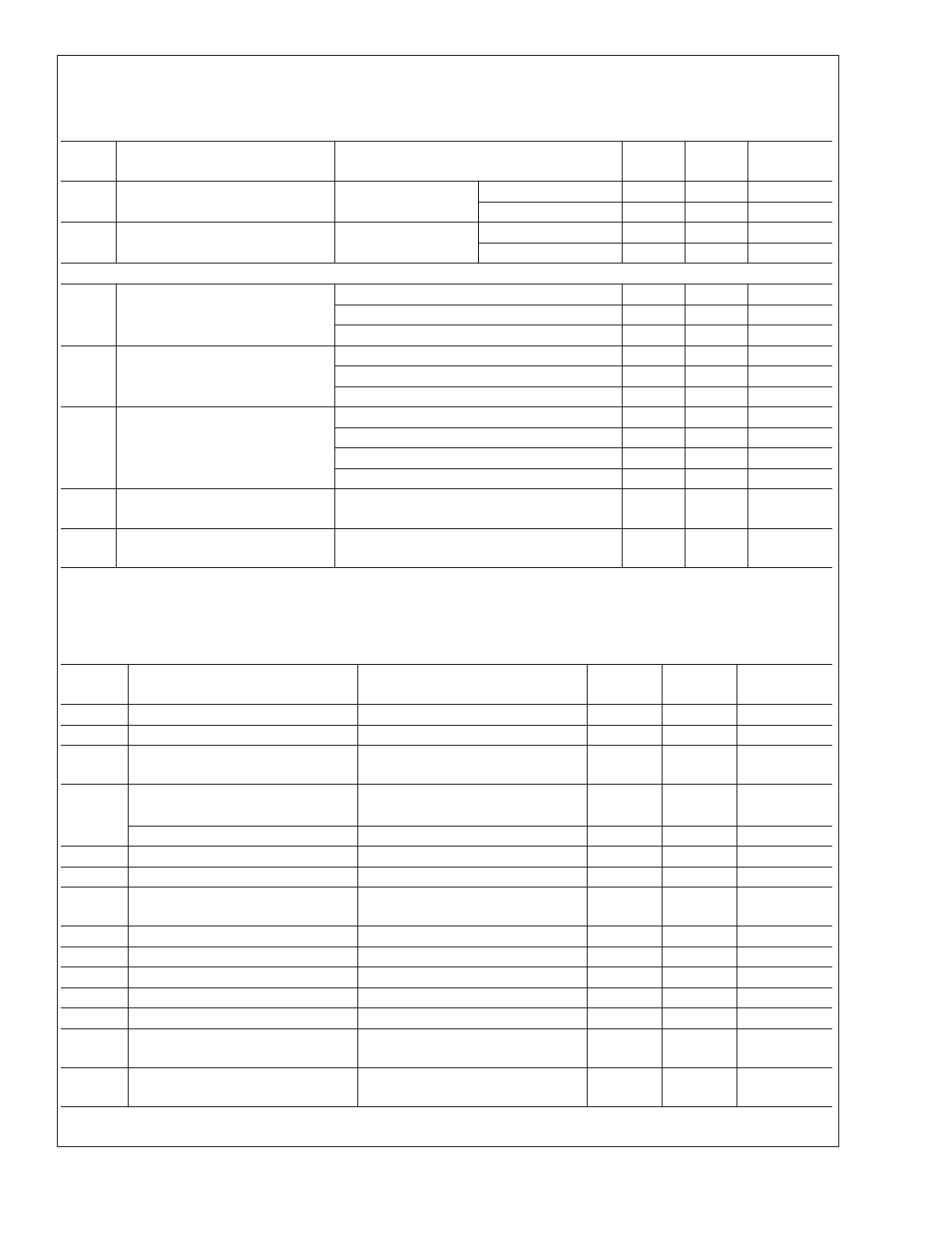
Converter Electrical Characteristics
(Continued)
The following specifications apply for V
A
= V
D
= V
DR
= +3.0 V
DC
, V
REF
= 1.0 V
DC
, GAIN = OF = 0V, OS = 3.0V, V
IN
(ac
coupled) = FSR = 1.0 V
P-P
, C
L
= 15 pF, f
CLK
= 20 MHz, 50% Duty Cycle, R
S
= 50
Ω
, t
rc
= t
fc
<
4 ns, NOT offset corrected.
Boldface limits apply for T
A
= T
MIN
to T
MAX
: all other limits T
A
= 25˚C (Note 7).
Symbol
Parameter
Conditions
Typical
Limits
Units
(Limits)
+I
SC
Output Short Circuit Source
Current
V
OUT
= 0V
Parallel Mode
−7
mA
Multiplexed Mode
−14
mA
−I
SC
Output Short Circuit Sink Current
V
OUT
= V
DR
Parallel Mode
7
mA
Multiplexed Mode
14
mA
POWER SUPPLY CHARACTERISTICS
I
A
+ I
D
Core Supply Current
PD = LOW, STBY = LOW, dc input
47.6
55
mA(max)
PD = LOW, STBY = HIGH
8.8
mA
PD = HIGH, STBY = LOW or HIGH
0.22
mA
I
DR
Digital Output Driver Supply
Current (Note 10)
PD = LOW, STBY = LOW, dc input
1.3
1.4
mA(max)
PD = LOW, STBY = HIGH
0.1
mA
PD = HIGH, STBY = LOW or HIGH
0.1
mA
PWR
Power Consumption
PD = LOW, STBY = LOW, dc input
150
169
mW(max)
PD = LOW, STBY = LOW, 1 MHz Input
178
mW
PD = LOW, STBY = HIGH
27
mW
PD = HIGH, STBY = LOW or HIGH
<
1
mW
PSRR1
Power Supply Rejection Ratio
Change in Full Scale with 2.7V to 3.6V Supply
Change
90
dB
PSRR2
Power Supply Rejection Ratio
Rejection at output with 20 MHz, 250 mV
P-P
Riding on V
A
and V
D
52
dB
AC Electrical Characteristics
OS = Low (Multiplexed Mode)
The following specifications apply for V
A
= V
D
= V
DR
= +3.0V
DC
, V
REF
= 1.0 V
DC
, GAIN = OF = 0V, OS = 0V, V
IN
(ac
coupled) = FSR = 1.0 V
P-P
, C
L
= 15 pF, f
CLK
= 20 MHz, 50% Duty Cycle, R
S
= 50
Ω
, t
rc
= t
fc
<
4 ns, NOT offset corrected.
Boldface limits apply for T
A
= T
MIN
to T
MAX
: all other limits T
A
= 25˚C (Note 7)
Symbol
Parameter
Conditions
Typical
Limits
Units
(Limits)
f
CLK1
Maximum Clock Frequency
30
20
MHz(min)
f
CLK2
Minimum Clock Frequency
1
MHz
Duty Cycle
50
30
70
%(min)
%(max)
Pipeline Delay (Latency)
I Data
2.5
Clock Cycles
Q Data
3.0
Clock Cycles
t
r
, t
f
Output Rise and Fall Times
4
ns
t
OC
Offset Correction Pulse Width
10
ns(min)
t
OD
Output Delay from CLK Edge to
Data Valid
13
18
ns(max)
t
DIQ
I/Q Output Delay
13
ns
t
SKEW
I/Q to Data Delay
±
200
ps
t
AD
Sampling (Aperture) Delay
2.4
ns
t
AJ
Aperture Jitter
<
10
ps(rms)
t
VALID
Data Valid Time
21
ns
Overrange Recovery Time
Differential V
IN
step from 1.5V to
0V
50
ns
t
WUPD
PD Low to 1/2 LSB Accurate
Conversion (Wake-Up Time)
<
1
ms
ADC10D020
www.national.com
9
