Pin descriptions and equivalent circuits – Rainbow Electronics ADC10D020 User Manual
Page 4
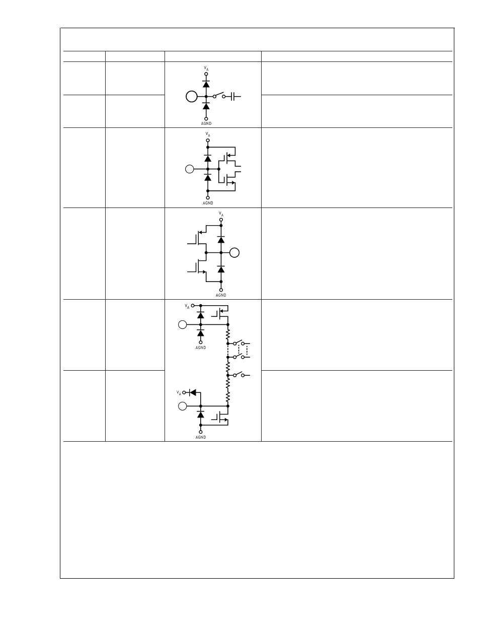
Pin Descriptions and Equivalent Circuits
Pin No.
Symbol
Equivalent Circuit
Description
48
47
I+
I−
Analog inputs to “I” ADC. Nominal conversion range is 1.25V
to 1.75V with GAIN pin low, or 1.0V to 2.0V with GAIN pin
high.
37
38
Q+
Q−
Analog inputs to “Q” ADC. Nominal conversion range is 1.25V
to 1.75V with GAIN pin low, or 1.0V to 2.0V with GAIN pin
high.
1
V
REF
Analog Reference Voltage input. The voltage at this pin
should be in the range of 0.8V to 1.5V. With 1.0V at this pin
and the GAIN pin
low, the full scale differential inputs are
1 V
P-P
. With 1.0V at this pin and the GAIN pin
high, the full
scale differential inputs are 2 V
P-P
. This pin should be
bypassed with a minimum 1 µF capacitor.
45
V
CMO
This is an analog output which can be used as a reference
source and/or to set the common mode voltage of the input. It
should be bypassed with a minimum of 1 µF low ESR
capacitor in parallel with a 0.1 µF capacitor. This pin has a
nominal output voltage of 1.5V and has a 1 mA output source
capability.
43
V
RP
Top of the reference ladder. Do not drive this pin. Bypass
this pin with a 10 µF low ESR capacitor and a 0.1 µF
capacitor.
44
V
RN
Bottom of the reference ladder. Do not drive this pin.
Bypass this pin with a 10 µF low ESR capacitor and a 0.1 µF
capacitor.
ADC10D020
www.national.com
4