Pin descriptions and equivalent circuits – Rainbow Electronics ADC10D020 User Manual
Page 5
Pin Descriptions and Equivalent Circuits
(Continued)
Pin No.
Symbol
Equivalent Circuit
Description
33
CLK
Digital clock input for both converters. The analog inputs are
sampled on the falling edge of this clock input.
2
OS
Output Bus Select. With this pin at a logic high, both the “I”
and the “Q” data are present on their respective 10-bit output
buses (Parallel mode of operation). When this pin is at a logic
low, the “I” and “Q” data are multiplexed onto the “I” output
bus and the “Q” output lines all remain at a logic low
(multiplexed mode).
31
OC
Offset Correct pin. A low-to-high transition on this pin initiates
an independent offset correction sequence for each converter,
which takes 34 clock cycles to complete. During this time 32
conversions are taken and averaged. The result is subtracted
from subsequent conversions. Each input pair should have 0V
differential value during this entire 34 clock period.
32
OF
Output Format pin. When this pin is LOW the output format is
Straight Binary. When this pin is HIGH the output format is 2’s
complement. This pin may be changed asynchronously, but
this will result in errors for one or two conversions.
34
STBY
Standby pin. The device operates normally with a logic low on
this and the PD (Power Down) pin. With this pin at a logic
high and the PD pin at a logic low, the device is in the
standby mode where it consumes just 27 mW of power. It
takes just 800 ns to come out of this mode after the STBY pin
is brought low.
35
PD
Power Down pin that, when high, puts the converter into the
Power Down mode where it consumes less than 1 mW of
power. It takes less than 1 ms to recover from this mode after
the PD pin is brought low. If both the STBY and PD pins are
high simultaneously, the PD pin dominates.
36
GAIN
This pin sets the internal signal gain at the inputs to the
ADCs. With this pin low the full scale differential input
peak-to-peak signal is equal to V
REF
. With this pin high the
full scale differential input peak-to-peak signal is equal to 2 x
V
REF
.
8 thru 27
I0–I9 and Q0–Q9
3V TTL/CMOS-compatible Digital Output pins that provide the
conversion results of the I and Q inputs. I0 and Q0 are the
LSBs, I9 and Q9 are the MSBs. Valid data is present just after
the rising edge of the CLK input in the Parallel mode. In the
multiplexed mode, I-channel data is valid on I0 through I9
when the I/Q output is high and the Q-channel data is valid
on I0 through I9 when the I/Q output is low.
28
I/Q
Output data valid signal. In the multiplexed mode, this pin
transitions from low to high when the data bus transitions
from Q-data to I-data, and from high to low when the data bus
transitions from I-data to Q-data. In the Parallel mode, this pin
transitions from low to high as the output data changes.
40, 41
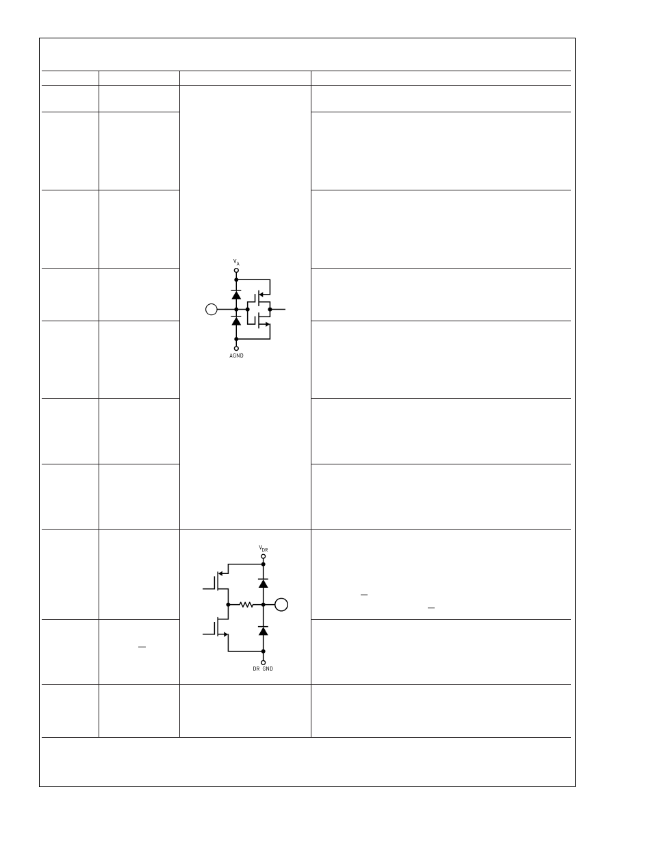
V
A
Positive analog supply pin. This pin should be connected to a
quiet voltage source of +2.7V to +3.6V. V
A
and V
D
should
have a common supply and be separately bypassed with
10 µF to 50 µF capacitors in parallel with 0.1 µF capacitors.
ADC10D020
www.national.com
5