0 power supply considerations, 0 layout and grounding, Figure 8. an acceptable layout pattern – Rainbow Electronics ADC10D020 User Manual
Page 30: Applications information

Applications Information
(Continued)
5.0 POWER SUPPLY CONSIDERATIONS
A/D converters draw sufficient transient current to corrupt
their own power supplies if not adequately bypassed. A
10 µF to 50 µF tantalum or aluminum electrolytic capacitor
should be placed within half an inch (1.2 centimeters) of the
A/D power pins, with a 0.1 µF ceramic chip capacitor placed
as close as possible to each of the converter’s power supply
pins. Leadless chip capacitors are preferred because they
have low lead inductance.
While a single voltage source should be used for the analog
and digital supplies of the ADC10D020, these supply pins
should be well isolated from each other to prevent any digital
noise from being coupled to the analog power pins. A choke
is recommended between the V
A
and V
D
supply lines. V
DR
should have a separate supply from V
A
and V
D
to avoid
noise coupling.
The V
DR
pins are completely isolated from the other supply
pins. Because of this isolation, a separate supply can be
used for these pins. This V
DR
supply can be significantly
lower than the three volts used for the other supplies, easing
the interface to lower voltage digital systems. Using a lower
voltage for this supply can also reduce the power consump-
tion and noise associated with the output drivers.
The converter digital supply should not be the supply that is
used for other digital circuitry on the board. It should be the
same supply used for the ADC10D020 analog supply.
As is the case with all high speed converters, the
ADC10D020 should be assumed to have little high fre-
quency power supply rejection. A clean analog power source
should be used.
No pin should ever have a voltage on it that is more than
300 mV in excess of the supply voltages or below ground,
not even on a transient basis. This can be a problem upon
application of power to a circuit and upon turn off of the
power source. Be sure that the supplies to circuits driving the
CLK, or any other digital or analog inputs do not come up
any faster than does the voltage at the ADC10D020 power
pins.
6.0 LAYOUT AND GROUNDING
Proper routing of all signals and proper ground techniques
are essential to ensure accurate conversion. Separate ana-
log and digital ground planes may be used if adequate care
is taken with signal routing, but may result in EMI/RFI. A
single ground plane with proper component placement will
yield good results while minimizing EMI/RFI.
Analog and digital ground current paths should not coincide
with each other as the common impedance will cause digital
noise to be added to analog signals. Accordingly, traces
carrying digital signals should be kept as far away from
traces carrying analog signals as is possible. Power should
be routed with traces rather than the use of a power plane.
The analog and digital power traces should be kept well
away from each other. All power to the ADC10D020, except
V
DR
, should be considered analog. The DR GND pin should
be considered a digital ground and not be connected to the
ground plane in close proximity with the other ground pins of
the ADC10D020.
Each bypass capacitor should be located as close to the
appropriate converter pin as possible and connected to the
pin and the appropriate ground plane with short traces. The
analog input should be isolated from noisy signal traces to
avoid coupling of spurious signals into the input. Any exter-
nal component (e.g., a filter capacitor) connected between
the converter’s input and ground should be connected to a
very clean point in the ground return.
The clock line should be properly terminated, as discussed
in Section 3.1, and be as short as possible.
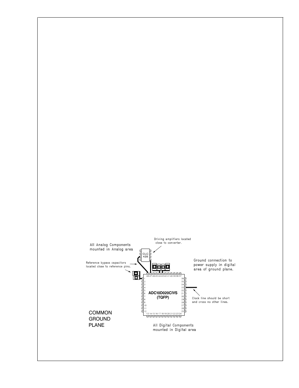
Figure 8 gives an example of a suitable layout and bypass
capacitor placement. All analog circuitry (input amplifiers,
filters, reference components, etc.) and interconnections
should be placed in an area reserved for analog circuitry. All
digital circuitry and I/O lines should be placed in an area
reserved for digital circuitry. Violating these rules can result
in digital noise getting into the analog circuitry, which will
degrade accuracy and dynamic performance (THD, SNR,
SINAD).
20025575
FIGURE 8. An Acceptable Layout Pattern
ADC10D020
www.national.com
30
