1 reference voltage, 2 vcmo output, 0 digital input pins – Rainbow Electronics ADC10D020 User Manual
Page 28: Applications information
Applications Information
(Continued)
2.1 REFERENCE VOLTAGE
The reference voltage should be within the range specified in
the Operating Ratings table (0.8V to 1.5V). A reference
voltage that is too low could result in a noise performance
that is less than desired because the quantization level falls
below other noise sources. On the other hand, a reference
voltage that is too high means that an input signal that
produces a full scale output uses such a large input range
that the input stage is less linear, resulting in a degradation
of distortion performance. Also, for large reference voltages,
the internal ladder buffer runs out of head-room, leading to a
reduction of gain in that buffer and causing gain error deg-
radation.
The Reference bypass pins V
RP
and V
RN
are output com-
pensated and should each be bypassed with a parallel com-
bination of a 5 µF (minimum) and 0.1 µF capacitors.
As mentioned in the previous section, the V
CMO
output can
be used as the ADC reference.
2.2 V
CMO
OUTPUT
The V
CMO
output pin is intended to provide a common mode
bias for the differential input pins of the ADC10D020. It can
also be used as a voltage reference source. Care should be
taken, however, to avoid loading this pin with more than 1
mA. A load greater than this could result in degraded long
term and temperature stability of this voltage. The V
CMO
pin
is output compensated and should be bypassed with a
2 µF/0.1 µF combination, minimum. See
INPUTS for more information on using the V
CMO
output as a
reference source.
3.0 DIGITAL INPUT PINS
The seven digital input pins are used to control the function
of the ADC10D020.
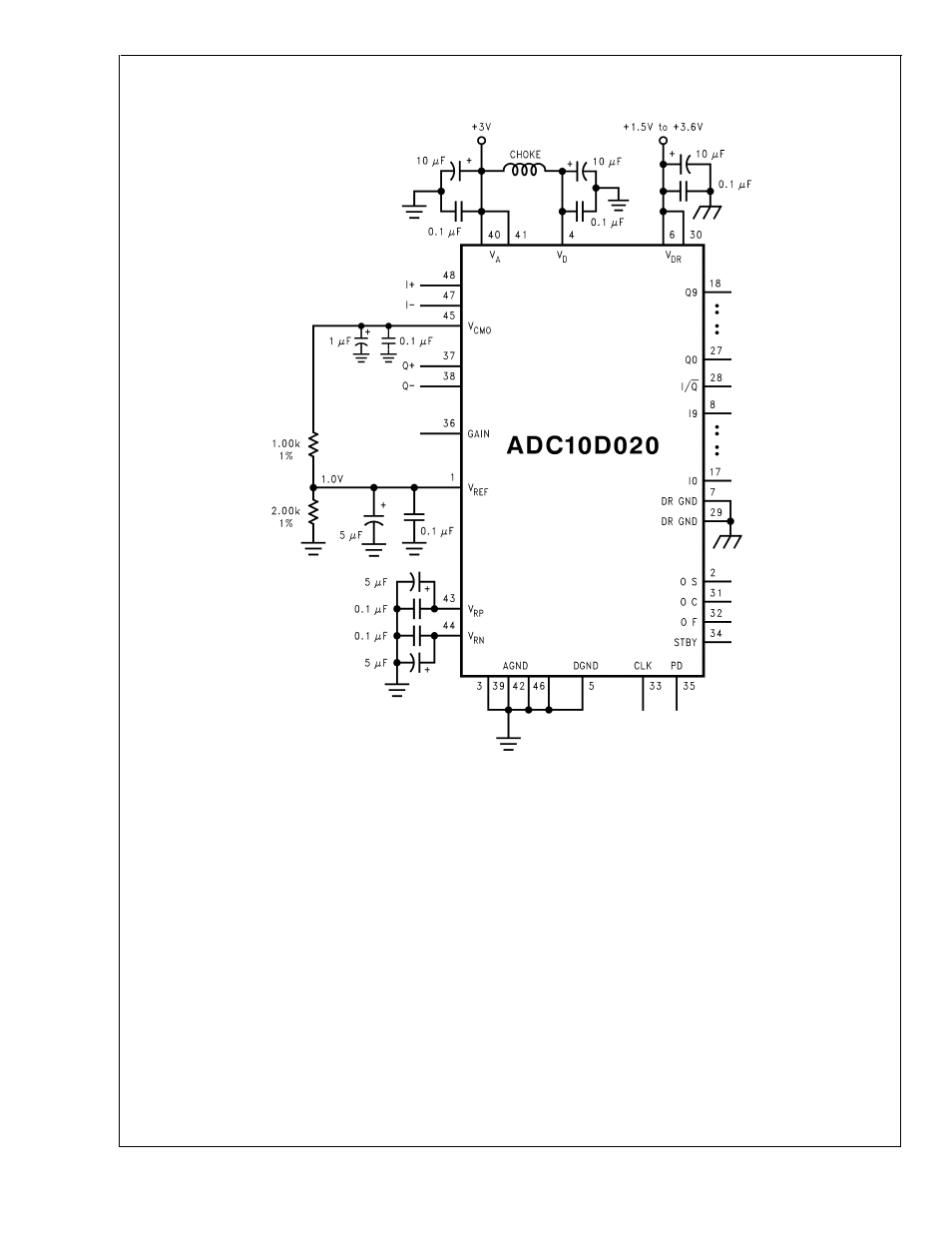
20025574
FIGURE 7. The V
CMO
output pin may be used as an internal reference source if its output is divided down and not
loaded excessively.
ADC10D020
www.national.com
28