Configuration register, Configuration register figure 8, Thermometer resolution configuration table 3 – Rainbow Electronics DS18B20X User Manual
Page 7: Resolution, Crc generation
DS18B20X
7 of 21
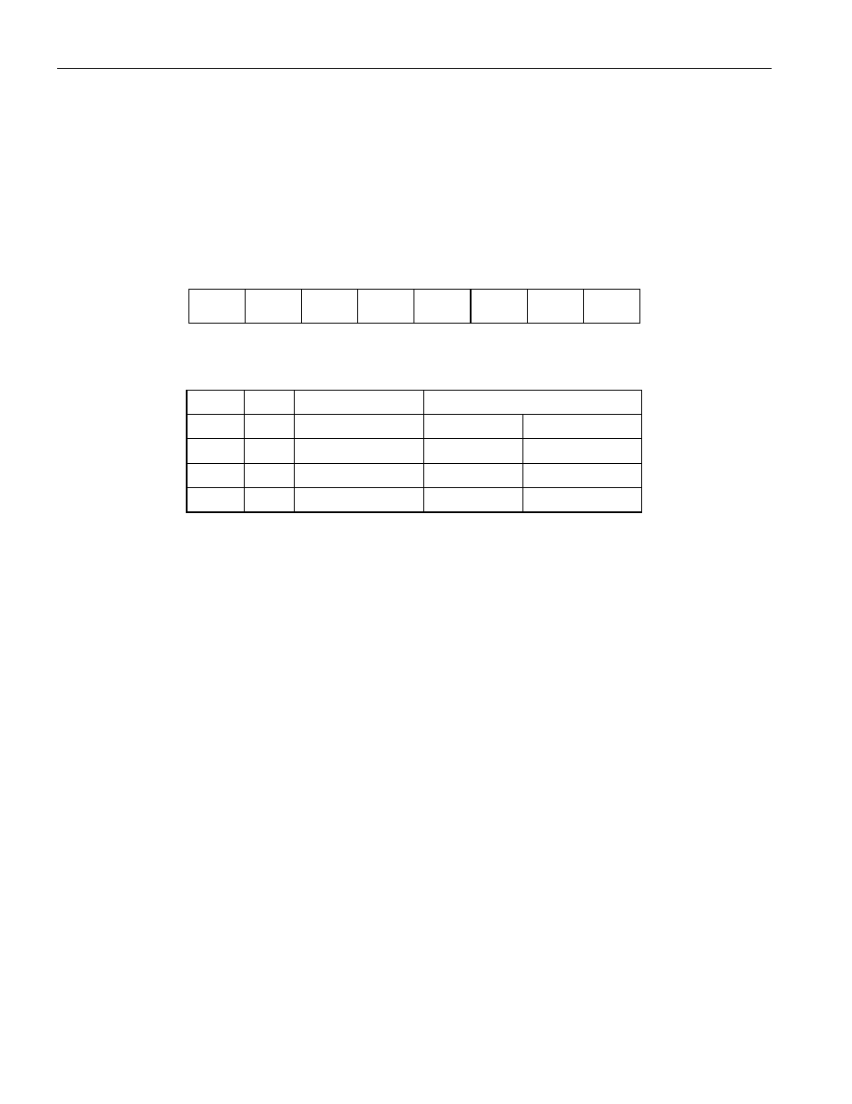
CONFIGURATION REGISTER
Byte 4 of the scratchpad memory contains the configuration register, which is organized as illustrated in
Figure 8. The user can set the conversion resolution of the DS18B20X using the R0 and R1 bits in this
register as shown in Table 3. The power-up default of these bits is R0 = 1 and R1 = 1 (12-bit resolution).
Note that there is a direct tradeoff between resolution and conversion time. Bit 7 and bits 0-4 in the
configuration register are reserved for internal use by the device and cannot be overwritten; these bits will
return 1s when read.
CONFIGURATION REGISTER Figure 8
bit 7
bit 6
bit 5
bit 4
bit 3
bit 2
bit 1
bit 0
0 R1
R0 1 1 1 1 1
THERMOMETER RESOLUTION CONFIGURATION Table 3
R1
R0
Resolution
Max Conversion Time
0 0
9-bit
93.75
ms (t
CONV
/8)
0 1
10-bit
187.5
ms (t
CONV
/4)
1 0
11-bit
375
ms (t
CONV
/2)
1 1
12-bit
750
ms
(t
CONV
)
CRC GENERATION
CRC bytes are provided as part of the DS18B20X’s 64-bit ROM code and in the 9
th
byte of the
scratchpad memory. The ROM code CRC is calculated from the first 56 bits of the ROM code and is
contained in the most significant byte of the ROM. The scratchpad CRC is calculated from the data
stored in the scratchpad, and therefore it changes when the data in the scratchpad changes. The CRCs
provide the bus master with a method of data validation when data is read from the DS18B20X. To
verify that data has been read correctly, the bus master must re-calculate the CRC from the received data
and then compare this value to either the ROM code CRC (for ROM reads) or to the scratchpad CRC (for
scratchpad reads). If the calculated CRC matches the read CRC, the data has been received error free. The
comparison of CRC values and the decision to continue with an operation are determined entirely by the
bus master. There is no circuitry inside the DS18B20X that prevents a command sequence from
proceeding if the DS18B20X CRC (ROM or scratchpad) does not match the value generated by the bus
master.
The equivalent polynomial function of the CRC (ROM or scratchpad) is:
CRC = X
8
+ X
5
+ X
4
+ 1
The bus master can re-calculate the CRC and compare it to the CRC values from the DS18B20X using
the polynomial generator shown in Figure 9. This circuit consists of a shift register and XOR gates, and
the shift register bits are initialized to 0. Starting with the least significant bit of the ROM code or the
least significant bit of byte 0 in the scratchpad, one bit at a time should shifted into the shift register.
After shifting in the 56
th
bit from the ROM or the most significant bit of byte 7 from the scratchpad, the
polynomial generator will contain the re-calculated CRC. Next, the 8-bit ROM code or scratchpad CRC
from the DS18B20X must be shifted into the circuit. At this point, if the re-calculated CRC was correct,