Detailed master read 1 timing figure 15, Recommended master read 1 timing figure 16, Related application notes – Rainbow Electronics DS18B20X User Manual
Page 16: And t
DS18B20X
16 of 21
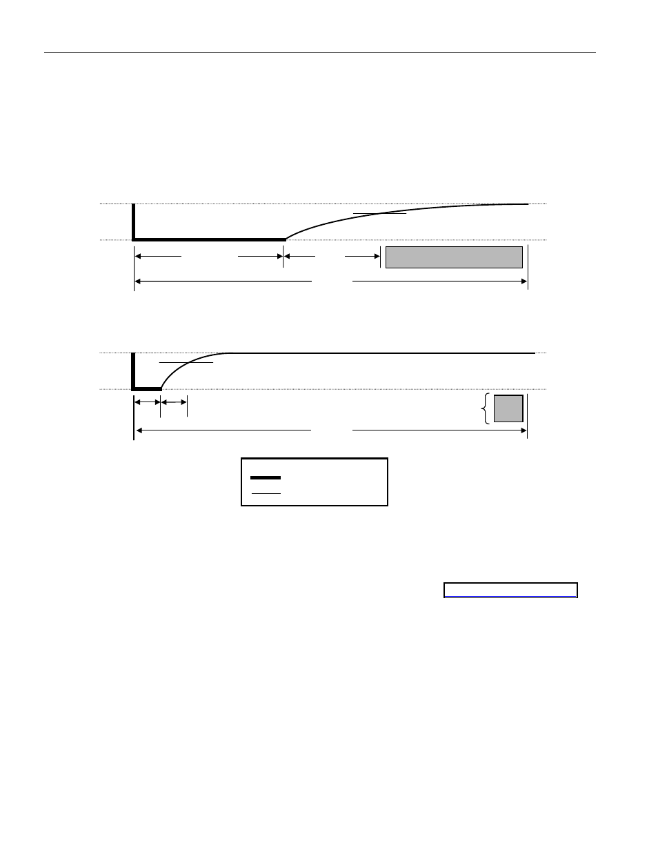
Therefore, the master must release the bus and then sample the bus state within 15
µ
s from the start of the
slot.
Figure 15 illustrates that the sum of T
INIT
, T
RC
, and T
SAMPLE
must be less than 15
µ
s for a read time slot.
Figure 16 shows that system timing margin is maximized by keeping T
INIT
and T
RC
as short as possible
and by locating the master sample time during read time slots towards the end of the 15
µ
s period.
DETAILED MASTER READ 1 TIMING Figure 15
RECOMMENDED MASTER READ 1 TIMING Figure 16
RELATED APPLICATION NOTES
The following Application Notes can be applied to the DS18B20X. These notes can be obtained from the
Dallas Semiconductor “Application Note Book,” via the Dallas website
through our faxback service at (214) 450–0441.
Application Note 27: “Understanding and Using Cyclic Redundancy Checks with Dallas Semiconductor
Touch Memory Product”
Application Note 55: “Extending the Contact Range of Touch Memories”
Application Note 74: “Reading and Writing Touch Memories via Serial Interfaces”
Application Note 104: “Minimalist Temperature Control Demo”
Application Note 106: “Complex MicroLANs”
Application Note 108: “MicroLAN – In the Long Run”
Sample 1-wire subroutines that can be used in conjunction with AN74 can be downloaded from the
Dallas website or anonymous FTP Site.
V
PU
GND
1-WIRE BUS
15
µµµµ
s
VIH of Master
T
RC
T
INT
> 1
µµµµ
s
Master samples
LINE TYPE LEGEND
Bus master pulling low
Resistor pullup
V
PU
GND
1-WIRE BUS
15
µµµµ
s
VIH of Master
T
RC
=
small
T
INT
=
small
Master samples