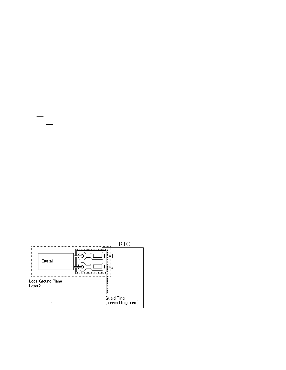
Signal descriptions, Typical pc board layout for crystal – Rainbow Electronics DS1339 User Manual
Page 3

DS1339
3 of 18
SIGNAL DESCRIPTIONS
V
CC
, GND – DC power is provided to the device on these pins.
SCL (Serial Clock Input) – SCL is used to synchronize data movement on the serial interface.
SDA (Serial Data Input/Output) – SDA is the input/output pin for the 2-wire serial interface. The SDA
pin is an open-drain output and requires an external pullup resistor.
V
BACKUP
(Secondary Supply Input) – Connection for a secondary power supply. Supply voltage must
be held between 1.3V and 3.7V for proper operation. This pin can be connected to a primary cell such as
a lithium button cell. Additionally, this pin can be connected to a rechargeable cell or a super cap when
used with the trickle charge feature.
SQW/
INT
(Square-Wave/Interrupt Output) – Programmable square-wave or interrupt-output signal.
The SQW/
INT
pin is an open-drain output and requires an external pullup resistor.
X1, X2 – These signals are connections for a standard 32.768kHz quartz crystal. The internal oscillator
circuitry is designed for operation with a crystal having a specified load capacitance (C
L
) of 6pF.
For more information about crystal selection and crystal layout considerations, refer to Application Note
58 “Crystal Considerations with Dallas Real-Time Clocks.”
The DS1339 can also be driven by an external 32.768kHz oscillator. In this configuration, the X1 pin is
connected to the external oscillator signal and the X2 pin is floated.
The oscillator is controlled by an enable bit in the control register. Oscillator startup times are highly
dependent upon crystal characteristics, PC board leakage, and layout. High ESR and excessive capacitive
loads are the major contributors to long startup times. A circuit using a crystal with the recommended
characteristics and proper layout usually starts within one second.
TYPICAL PC BOARD LAYOUT FOR CRYSTAL
