Application circuits – Rainbow Electronics ICL7660 User Manual
Page 9
The first term is the effective resistance from the
switched-capacitor circuit.
Conversion losses occur during the transfer of charge
between capacitors C1 and C2 when there is a voltage
difference between them. The power loss is:
Increasing Efficiency
Efficiency can be improved by lowering output voltage
ripple and output impedance. Both output voltage rip-
ple and output impedance can be reduced by using
large capacitors with low ESR.
The output voltage ripple can be calculated by noting
that the output current is supplied solely from capacitor
C2 during one-half of the charge-pump cycle.
Slowing the oscillator frequency reduces quiescent cur-
rent. The oscillator frequency can be reduced by con-
necting a capacitor to the OSC pin.
Reducing the oscillator frequency increases the ripple
voltage in the MAX1044/ICL7660. Compensate by
increasing the values of the bucket and reservoir
capacitors. For example, in a negative voltage converter,
the pump frequency is around 4kHz or 5kHz. With the
recommended 10µF bucket and reservoir capacitors,
the circuit consumes about 70µA of quiescent current
while providing 20mA of output current. Setting the
oscillator to 400Hz by connecting a 100pF capacitor to
OSC reduces the quiescent current to about 15µA.
Maintaining 20mA output current capability requires
increasing the bucket and reservoir capacitors to
100µF.
Note that lower capacitor values can be used for lower
output currents. For example, setting the oscillator to
40Hz by connecting a 1000pF capacitor to OSC pro-
vides the highest efficiency possible. Leaving the bucket
and reservoir capacitors at 100µF gives a maximum
I
OUT
of 2mA, a no-load quiescent current of 10µA, and
a power conversion efficiency of 98%.
General Precautions
1) Connecting any input terminal to voltages greater
than V+ or less than ground may cause latchup. Do
not apply any input sources operating from external
supplies before device power-up.
2) Never exceed maximum supply voltage ratings.
3) Do not connect C1 and C2 with the wrong polarity.
4) Do not short V+ to ground for extended periods with
supply voltages above 5.5V present on other pins.
5) Ensure that V
OUT
(pin 5) does not go more positive
than GND (pin 3). Adding a diode in parallel with
C2, with the anode connected to V
OUT
and cathode
to LV, will prevent this condition.
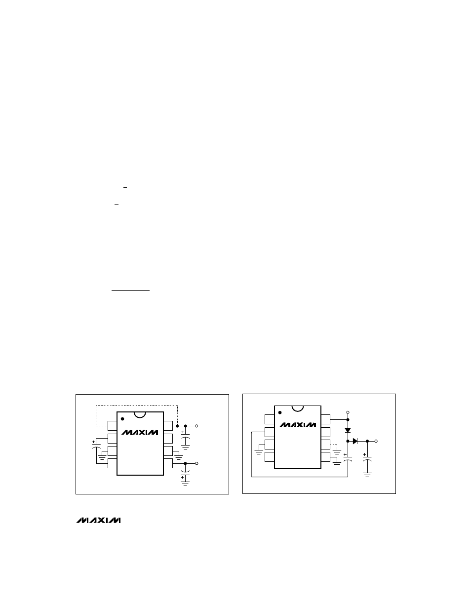
________________Application Circuits
Negative Voltage Converter
Figure 8 shows a negative voltage converter, the most
popular application of the MAX1044/ICL7660. Only two
external capacitors are needed. A third power-supply
bypass capacitor is recommended (0.1µF to 10µF)
V
1
2 x f
x C2
2 x ESR
I
RIPPLE
OSC
C2
OUT
≅
+
P
1
2
C1 (V
V
1
2
C2 V
2V
V
x f
/ 2
CONV.LOSS
OUT
2
RIPPLE
2
OUT RIPPLE
OSC
)
=
+
−
+
−
2
MAX1044/ICL7660
Switched-Capacitor Voltage Converters
_______________________________________________________________________________________
9
MAX1044
ICL7660
4
3
C1
10µF
V
OUT
=
-(V+)
C
BYPASS
0.1µF
2
1
5
6
7
8
C2
10µF
V+
BOOST
LV
Figure 8. Negative Voltage Converter with BOOST and LV
Connections
MAX1044
ICL7660
4
3
V
OUT
= 2(V+) - 2V
D
2
1
5
6
7
8
C1
C2
V+
Figure 9. Voltage Doubler