Detailed description, Pin description – Rainbow Electronics ICL7660 User Manual
Page 5
_______________Detailed Description
The MAX1044/ICL7660 are charge-pump voltage con-
verters. They work by first accumulating charge in a
bucket capacitor and then transfer it into a reservoir
capacitor. The ideal voltage inverter circuit in Figure 2
illustrates this operation.
During the first half of each cycle, switches S1 & S3
close and switches S2 & S4 open, which connects the
bucket capacitor C1 across V+ and charges C1.
During the second half of each cycle, switches S2 & S4
close and switches S1 & S3 open, which connects the
positive terminal of C1 to ground and shifts the nega-
tive terminal to V
OUT
. This connects C1 in parallel with
the reservoir capacitor C2. If the voltage across C2 is
smaller than the voltage across C1, then charge flows
from C1 to C2 until the voltages across them are equal.
During successive cycles, C1 will continue pouring
charge into C2 until the voltage across C2 reaches
- (V+). In an actual voltage inverter, the output is less
than - (V+) since the switches S1–S4 have resistance
and the load drains charge from C2.
Additional qualities of the MAX1044/ICL7660 can be
understood by using a switched-capacitor circuit
model. Switching the bucket capacitor, C1, between
the input and output of the circuit synthesizes a resis-
tance (Figures 3a and 3b.)
When the switch in Figure 3a is in the left position,
capacitor C1 charges to V+. When the switch moves to
the right position, C1 is discharged to V
OUT
. The
charge transferred per cycle is:
∆
Q = C1(V+ - V
OUT
). If
the switch is cycled at frequency f, then the resulting
MAX1044/ICL7660
Switched-Capacitor Voltage Converters
_______________________________________________________________________________________
5
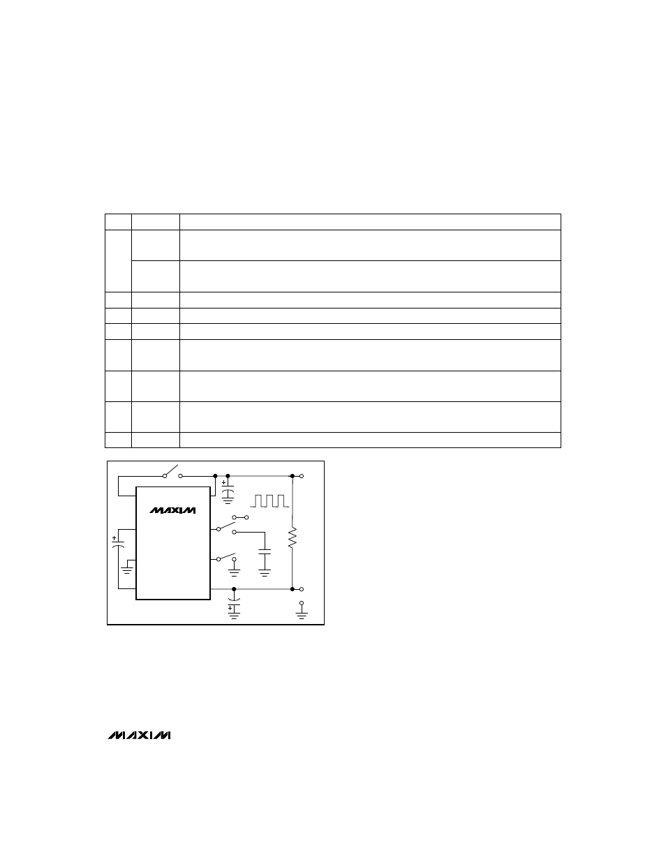
MAX1044
ICL7660
BOOST
CAP+
GND
C
BYPASS
= 0.1µF
V+
R
L
CAP-
V+
OSC
C1
10
µ
F
LV
V
OUT
C2
10
µ
F
C
OSC
EXTERNAL
OSCILLATOR
V
OUT
_____________________________________________________________ Pin Description
NAME
FUNCTION
BOOST
(MAX1044)
Frequency Boost. Connecting BOOST to V+ increases the oscillator frequency by a factor of six. When the
oscillator is driven externally, BOOST has no effect and should be left open.
PIN
1
N.C.
(ICL7660)
No Connection
3
GND
Ground. For most applications, the positive terminal of the reservoir capacitor is connected to this pin.
2
CAP+
Connection to positive terminal of Charge-Pump Capacitor
6
LV
Low-Voltage Operation. Connect to ground for supply voltages below 3.5V.
ICL7660: Leave open for supply voltages above 5V.
5
V
OUT
Negative Voltage Output. For most applications, the negative terminal of the reservoir capacitor is
connected to this pin.
4
CAP-
Connection to negative terminal of Charge-Pump Capacitor
7
OSC
Oscillator Control Input. Connecting an external capacitor reduces the oscillator frequency. Minimize stray
capacitance at this pin.
8
V+
Power-Supply Positive Voltage Input. (1.5V to 10V). V+ is also the substrate connection.
Figure 1. Maxim MAX1044/ICL7660 Test Circuit