Rainbow Electronics MAX4492 User Manual
Page 6

pole at frequency (2
πR′C
IN
)
-1
, where R
′ is the parallel
combination of the gain-setting resistors for the invert-
ing or noninverting amplifier configuration (Figure 2). If
the pole frequency is less than or comparable to the
unity-gain bandwidth (10MHz), the phase margin will
be reduced, and the amplifier will exhibit degraded
AC performance through either ringing in the step
response or sustained oscillations. The pole frequency is
10MHz when R
′ = 3.2kΩ. To maximize stability, R′ <3kΩ
is recommended.
Applications that require rail-to-rail operation with mini-
mal loading (for small V
DD
- V
OH
and V
OL
- V
SS
) will
typically require R
′ values >3kΩ. To improve step
response under these conditions, connect a small
capacitor C
f
between the inverting input and output.
Choose C
f
as follows:
C
f
= 5(R / R
f
) [pf]
where R
f
is the feedback resistor and R is the gain-set-
ting resistor (Figure 2).
Figure 3 shows the step response for a noninverting
amplifier subject to R
′ = 4kΩ with and without the C
f
feedback capacitor.
MAX4490/MAX4491/MAX4492
Low-Cost, High-Slew-Rate,
Rail-to-Rail I/O Op Amps in SC70
6
_______________________________________________________________________________________
Figure 1a. Output Source Current vs. Temperature
Figure 1b. Output Sink Current vs. Temperature
0
1
2
3
4
5
6
-40
-10
-25
5
20 35 50 65 80
125
95 110
TEMPERATURE (
°C)
OUTPUT SOURCE CURRENT (mA)
V
DD
- V
OH
= 200mV
V
DD
- V
OH
= 100mV
V
DD
- V
OH
= 50mV
V
DD
= 5V
V
DD
= 2.7V
0
1
2
3
4
5
6
7
8
9
-40
-10
-25
5
20 35
65
50
80
110
95
125
TEMPERATURE (
°C)
OUTPUT SINK CURRENT (mA)
V
DD
- V
OH
= 200mV
V
DD
- V
OH
= 100mV
V
DD
- V
OH
= 50mV
V
DD
= 5V
V
DD
= 2.7V
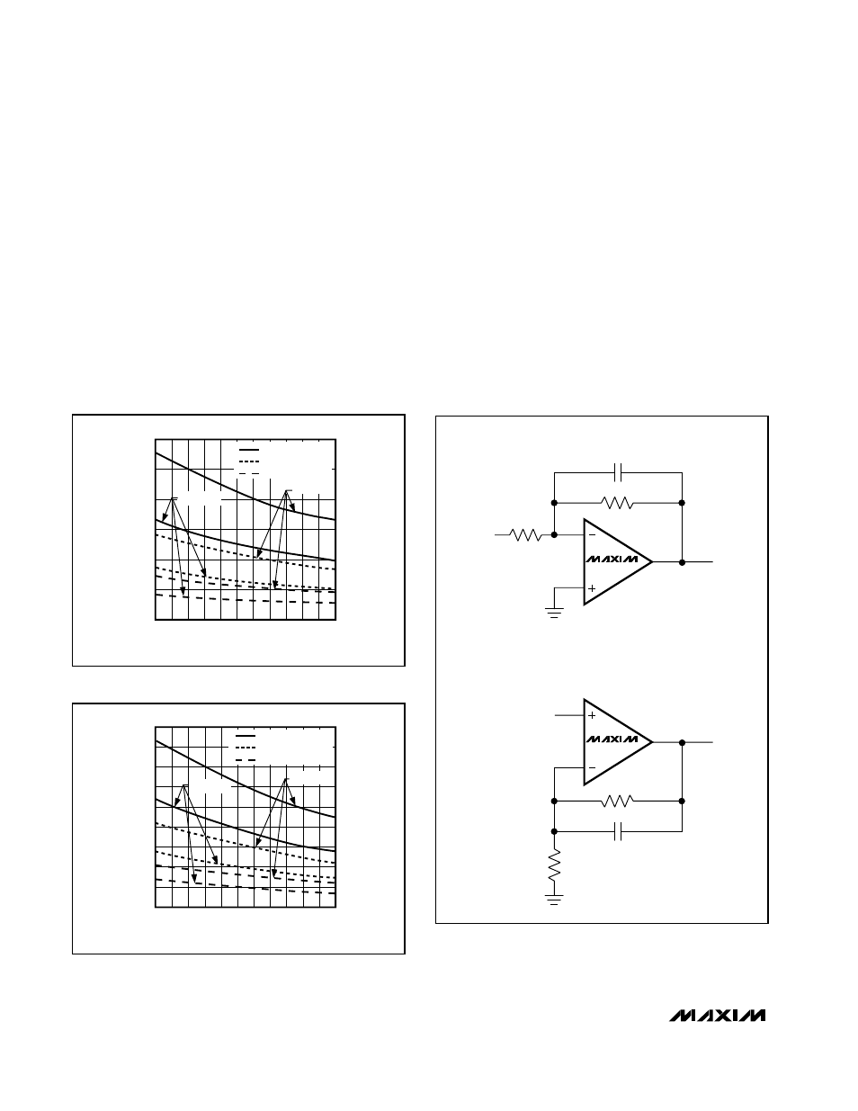
Figure 2. Inverting and Noninverting Amplifier with Feedback
Compensation
MAX4490
V
IN
V
OUT
R
′ = R || R
f
R
f
C
f
= RC
IN
R
f
C
f
R
MAX4490
V
IN
V
OUT
R
′ = R || R
f
R
f
C
f
= RC
IN
R
f
R
C
f
INVERTING
NONINVERTING
