Rainbow Electronics MAX4492 User Manual
Page 2
MAX4490/MAX4491/MAX4492
Low-Cost, High-Slew-Rate,
Rail-to-Rail I/O Op Amps in SC70
2
_______________________________________________________________________________________
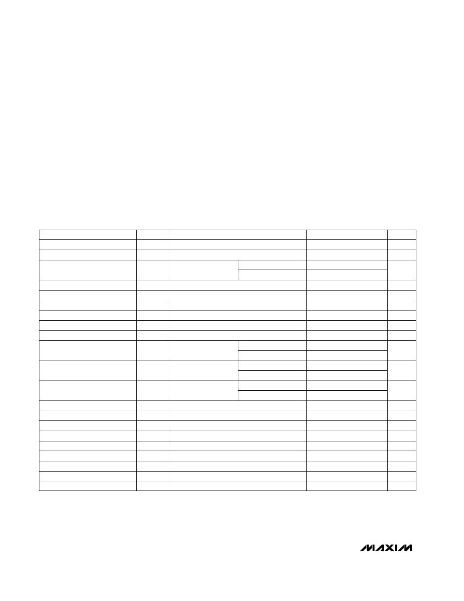
ABSOLUTE MAXIMUM RATINGS
ELECTRICAL CHARACTERISTICS
(V
DD
= 5V, V
SS
= 0, V
CM
= 0, V
OUT
= V
DD
/2, R
L
= 100k
Ω connected to V
DD
/2, T
A
= T
MIN
to T
MAX
, unless otherwise noted. Typical
values are at T
A
= +25°C.) (Note 1)
Stresses beyond those listed under “Absolute Maximum Ratings” may cause permanent damage to the device. These are stress ratings only, and functional
operation of the device at these or any other conditions beyond those indicated in the operational sections of the specifications is not implied. Exposure to
absolute maximum rating conditions for extended periods may affect device reliability.
Supply Voltage (V
DD
to V
SS
) ....................................................6V
All Other Pins ...................................(V
SS
- 0.3V) to (V
DD
+ 0.3V)
Output Short-Circuit Duration .................................................10s
Continuous Power Dissipation (T
A
= +70°C)
5-Pin SC70 (derate 2.5mW/°C above +70°C) ............ 200mW
5-Pin SOT23 (derate 7.1mW/°C above +70°C).......... 571mW
8-Pin SOT23 (derate 5.26mW/°C above +70°C)........421 mW
8-Pin µMAX (derate 4.1mW/°C above +70°C) ........... 330mW
14-Pin TSSOP (derate 8.3mW/°C above +70°C) ....... 667mW
14-Pin SO (derate 8.3mW/°C above +70°C).............. 667mW
Operating Temperature Range ........................ -40°C to +125°C
Junction Temperature ..................................................... +150°C
Storage Temperature Range ............................ -65°C to +150°C
Lead Temperature (soldering, 10s) ................................ +300°C
A
V(CL)
= 1, no sustained oscillations
ƒ = 10kHz
T
A
= +25°C
ƒ = 10kHz
Measured from 10% to 90% of 4V
P-P
step
(Note 2)
C
L
= 10pF
C
L
= 10pF
R
L
= 100k
Ω
2.7V
≤ V
DD
≤ 5.5V
C
L
= 10pF
V
SS
≤ V
CM
≤ V
DD
Inferred from CMRR test
T
A
= T
MIN
to T
MAX
(Note 3)
(Note 3)
Sourcing or sinking
R
L
= 2k
Ω
CONDITIONS
pF
300
Capacitive-Load Drive
fA
√
Hz
1
i
n
Current-Noise Density
nV/
√
Hz
12
e
n
Voltage-Noise Density
V/µs
10
SR
Slew Rate
dB
10
Gain Margin
degrees
60
Phase Margin
pF
5
C
IN
Input Capacitance
MHz
10
GBWP
Gain-Bandwidth Product
mA
±50
I
OUT(SC)
Output Short-Circuit Current
65
85
mV
±1.5
±10
V
OS
Input Offset Voltage
mA
0.8
2
I
S
V
2.7
5.5
V
DD
Supply Voltage Range
Supply Current (per amplifier)
dB
110
A
V
Large-Signal Voltage Gain
dB
65
100
PSRR
Power-Supply Rejection Ratio
dB
54
75
CMRR
Common-Mode Rejection Ratio
V
V
SS
V
DD
V
CM
Input Common-Mode Range
16
nA
±0.05
±2.5
I
B
Input Bias Current
nA
±0.05
±2.5
I
OS
Input Offset Current
M
Ω
1000
R
IN
Input Resistance
UNITS
MIN
TYP
MAX
SYMBOL
PARAMETER
Note 1: All units production tested at T
A
= +25°C. Limits over temperature guaranteed by design.
Note 2: Guaranteed by the Power-Supply Rejection Ratio (PSRR) test.
Note 3: Input Offset Voltage, Input Bias Current, and Input Offset Current are all tested and guaranteed at both ends of the common-
mode range.
(V
SS
+ 0.25V)
≤ V
OUT
≤ (V
DD
- 0.25V)
R
L
= 100k
Ω
R
L
= 2k
Ω
55
200
mV
1.5
V
OH
Output-Voltage Swing High
Specified as
V
DD
- V
OH
R
L
= 100k
Ω
R
L
= 2k
Ω
35
150
mV
1.5
V
OL
Output-Voltage Swing Low
Specified as
V
OL
- V
SS
(Note 3)