Pin description, Detailed description, Applications information – Rainbow Electronics MAX4492 User Manual
Page 5
MAX4490/MAX4491/MAX4492
Low-Cost, High-Slew-Rate,
Rail-to-Rail I/O Op Amps in SC70
_______________________________________________________________________________________
5
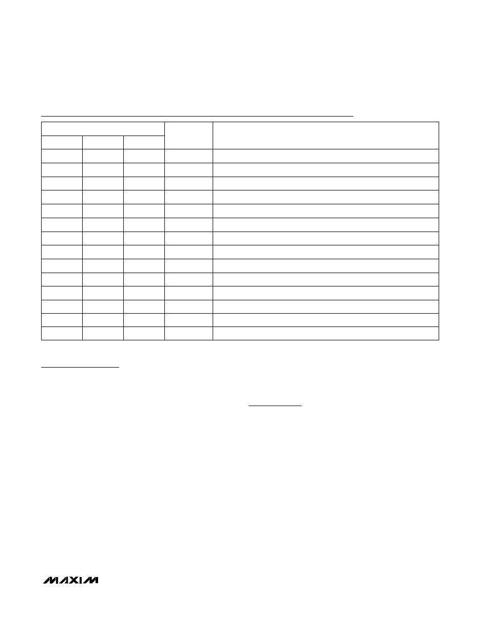
NAME
FUNCTION
MAX4490
1
IN+
Noninverting Input
PIN
2
V
SS
Negative Supply Input. Connect to ground for single-supply operation.
3
IN-
Inverting Input
—
INA-
Inverting Input to Amplifier A
—
INA+
Noninverting Input to Amplifier A
5
V
DD
Positive Supply Input
4
OUT
Amplifier Output
—
INC+, IND+
Noninverting Inputs to Amplifiers C and D
—
OUTB
Amplifier B Output
—
INB-
Inverting Input to Amplifier B
—
INB+
Noninverting Input to Amplifier B
—
OUTA
Amplifier A Output
Pin Description
MAX4492
—
11
—
2
3
4
—
10, 12
7
6
5
1
MAX4491
—
4
—
2
3
8
—
—
7
6
5
1
—
—
9, 13
INC-, IND-
Inverting Inputs to Amplifiers C and D
—
—
8, 14
OUTC, OUTD
Amplifiers C and D Outputs
Detailed Description
Rail-to-Rail Input Stage
The MAX4490/MAX4491/MAX4492 CMOS operational
amplifiers have parallel-connected N- and P-channel
differential input stages that combine to accept a com-
mon-mode range extending to both supply rails. The N-
channel stage is active for common-mode input
voltages typically greater than (V
SS
+ 1.2V), and the P-
channel stage is active for common-mode input volt-
ages typically less than (V
DD
- 1.2V).
Rail-to-Rail Output Stage
The MAX4490/MAX4491/MAX4492 CMOS operational
amplifiers feature class-AB push-pull output stages that
can drive a 100k
Ω load to within 1.5mV of either supply
rail. Short-circuit output current is typically ±50mA.
Figures 1a and 1b show the typical temperature depen-
dence of output source and sink currents, respectively,
for three fixed values of (V
DD
- V
OH
) and (V
OL
- V
SS
).
For example, at V
DD
= 5.0V, the load currents that main-
tain (V
DD
- V
OH
) = 100mV and (V
OL
- V
SS
) = 100mV at
T
A
= +25°C are 2.2mA and 3.3mA, respectively, when
the load is connected to V
DD
/2. Consistent resistive-
drive capability is (2.5 - 0.1) / 2.2 = 1.1k
Ω. For the same
application, resistive-drive capability is 2.2k
Ω when the
load is connected to V
DD
or V
SS
.
Applications Information
Power-Supply Considerations
The MAX4490/MAX4491/MAX4492 operate from a sin-
gle 2.7V to 5.5V supply or from dual ±1.35V to ±2.75V
supplies with typically 800µA supply current per ampli-
fier. A high power-supply rejection ratio of 100dB
allows for extended operation from a decaying battery
voltage, thereby simplifying designs for portable appli-
cations. For single-supply operation, bypass the power
supply with a 0.1µF ceramic capacitor placed close to
the V
DD
pin. For dual-supply operation, bypass each
supply to ground.
Input Capacitance
One consequence of the parallel-connected differential
input stages for rail-to-rail operation is a relatively large
input capacitance C
IN
(typically 5pF). This introduces a