Applications information – Rainbow Electronics MAX4040_MAX4044 User Manual
Page 9
MAX4040–MAX4044
Single/Dual/Quad, Low-Cost, SOT23,
Micropower, Rail-to-Rail I/O Op Amps
_______________________________________________________________________________________
9
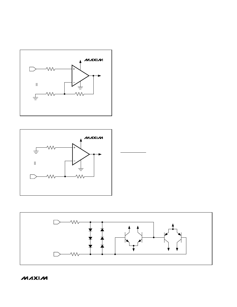
The MAX4040–MAX4044 family’s inputs are protected
from large differential input voltages by internal 2.2k
Ω
series resistors and back-to-back triple-diode stacks
across the inputs (Figure 2). For differential input volt-
ages (much less than 1.8V), input resistance is typically
45M
Ω
. For differential input voltages greater than 1.8V,
input resistance is around 4.4k
Ω
, and the input bias
current can be approximated by the following equation:
I
BIAS
= (V
DIFF
- 1.8V) / 4.4k
Ω
In the region where the differential input voltage
approaches 1.8V, the input resistance decreases expo-
nentially from 45M
Ω
to 4.4k
Ω
as the diode block begins
conducting. Conversely, the bias current increases with
the same curve.
Rail-to-Rail Output Stage
The MAX4040–MAX4044 output stage can drive up to a
25k
Ω
load and still swing to within 60mV of the rails.
Figure 3 shows the output voltage swing of a MAX4040
configured as a unity-gain buffer, powered from a single
+4.0V supply voltage. The output for this setup typically
swings from (V
EE
+ 10mV) to (V
CC
- 10mV) with a 100k
Ω
load.
Applications Information
Power-Supply Considerations
The MAX4040–MAX4044 operate from a single +2.4V to
+5.5V supply (or dual ±1.2V to ±2.75V supplies) and
consume only 10µA of supply current per amplifier. A
high power-supply rejection ratio of 85dB allows the
amplifiers to be powered directly off a decaying battery
voltage, simplifying design and extending battery life.
Power-Up Settling Time
The MAX4040–MAX4044 typically require 200µs to
power up after V
CC
is stable. During this start-up time,
the output is indeterminant. The application circuit
should allow for this initial delay.
R3
R3 = R1 R2
R1
R2
MAX4040–
MAX4044
V
IN
Figure 1b. Minimizing Offset Error Due to Input Bias Current
(Inverting)
2.2k
2.2k
IN-
IN+
Figure 2. Input Protection Circuit
R3
V
IN
R3 = R1 R2
R1
R2
MAX4040–
MAX4044
Figure 1a. Minimizing Offset Error Due to Input Bias Current
(Noninverting)