Rainbow Electronics MAX4040_MAX4044 User Manual
Page 11
MAX4040–MAX4044
Single/Dual/Quad, Low-Cost, SOT23,
Micropower, Rail-to-Rail I/O Op Amps
______________________________________________________________________________________
11
For example, a MAX4040 running from a single +2.4V
supply, operating at T
A
= +25°C, can source 240µA to
within 100mV of V
CC
and is capable of driving a 9.6k
Ω
load resistor to V
EE
:
The same application can drive a 4.6k
Ω
load resistor
when terminated in V
CC
/ 2 (+1.2V in this case).
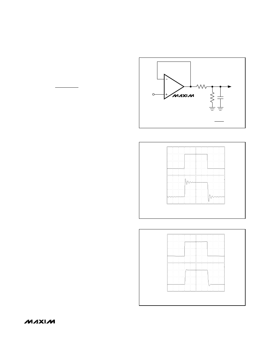
Driving Capacitive Loads
The MAX4040–MAX4044 are unity-gain stable for loads
up to 200pF (see Load Resistor vs. Capacitive Load
graph in
Typical Operating Characteristics
).
Applications that require greater capacitive drive capa-
bility should use an isolation resistor between the output
and the capacitive load (Figures 6a–6c). Note that this
alternative results in a loss of gain accuracy because
R
ISO
forms a voltage divider with the load resistor.
Power-Supply Bypassing and Layout
The MAX4040–MAX4044 family operates from either a
single +2.4V to +5.5V supply or dual ±1.2V to ±2.75V
supplies. For single-supply operation, bypass the
power supply with a 100nF capacitor to V
EE
(in this
case GND). For dual-supply operation, both the V
CC
and V
EE
supplies should be bypassed to ground with
separate 100nF capacitors.
Good PC board layout techniques optimize perfor-
mance by decreasing the amount of stray capacitance
at the op amp’s inputs and output. To decrease stray
capacitance, minimize trace lengths by placing exter-
nal components as close as possible to the op amp.
Surface-mount components are an excellent choice.
Using the MAX4040–MAX4044
as Comparators
Although optimized for use as operational amplifiers,
the MAX4040–MAX4044 can also be used as rail-to-rail
I/O comparators. Typical propagation delay depends
on the input overdrive voltage, as shown in Figure 7.
External hysteresis can be used to minimize the risk of
output oscillation. The positive feedback circuit, shown
in Figure 8, causes the input threshold to change when
the output voltage changes state. The two thresholds
create a hysteresis band that can be calculated by the
following equations:
V
HYST
= V
HI
- V
LO
V
LO
= V
IN
x R2 / (R1 + (R1 x R2 / R
HYST
) + R2)
V
HI
= [(R2 / R1 x V
IN
) + (R2 / R
HYST
) x V
CC
] /
(1 + R1 / R2 + R2 / R
HYST
)
R =
2.4V - 0.1V
240 A
9.6k to V
L
EE
µ
=
Ω
50mV/div
IN
OUT
50mV/div
MAX4040/42/44 fig06b
100
µ
s/div
R
ISO
= NONE, R
L
= 100k
Ω
, C
L
= 700pF
Figure 6b. Pulse Response without Isolating Resistor
50mV/div
IN
OUT
50mV/div
MAX4040/42/44 fig06c
100
µ
s/div
R
ISO
= 1k
Ω
, R
L
= 100k
Ω
, C
L
= 700pF
Figure 6c. Pulse Response with Isolating Resistor
R
ISO
C
L
R
L
MAX4040–
MAX4044
A
V
=
R
L
≈
1
R
L
+ R
ISO
Figure 6a. Using a Resistor to Isolate a Capacitive Load from
the Op Amp