Rainbow Electronics MAX4040_MAX4044 User Manual
Page 12
MAX4040–MAX4044
Single/Dual/Quad, Low-Cost, SOT23,
Micropower, Rail-to-Rail I/O Op Amps
12
______________________________________________________________________________________
The MAX4040–MAX4044 contain special circuitry to
boost internal drive currents to the amplifier output
stage. This maximizes the output voltage range over
which the amplifiers are linear. In an open-loop com-
parator application, the excursion of the output voltage
is so close to the supply rails that the output stage tran-
sistors will saturate, causing the quiescent current to
increase from the normal 10µA. Typical quiescent cur-
rents increase to 35µA for the output saturating at V
CC
and 28µA for the output at V
EE
.
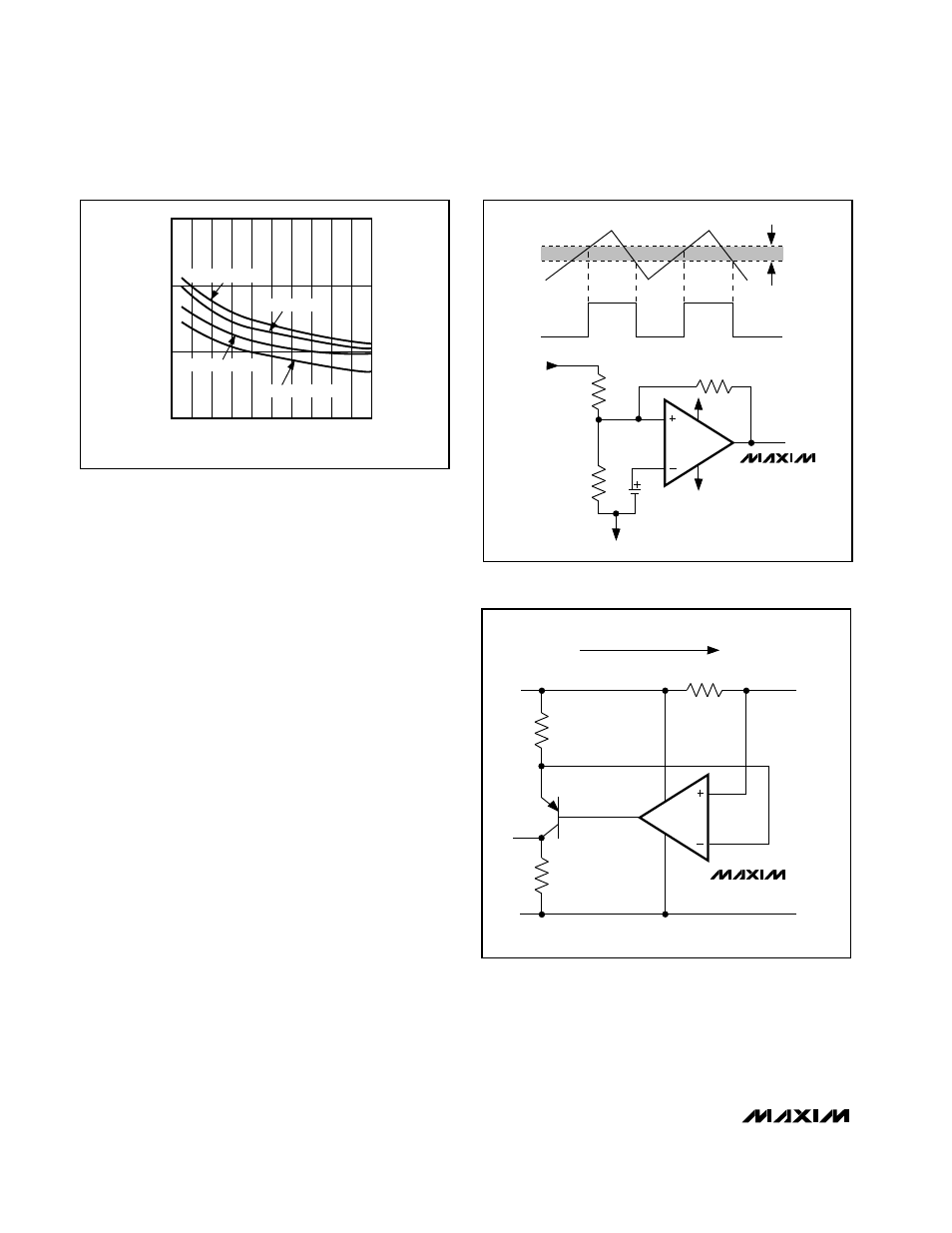
Using the MAX4040–MAX4044
as Ultra-Low-Power Current Monitors
The MAX4040–MAX4044 are ideal for applications pow-
ered from a battery stack. Figure 9 shows an application
circuit in which the MAX4040 is used for monitoring the
current of a battery stack. In this circuit, a current load is
applied, and the voltage drop at the battery terminal is
sensed.
The voltage on the load side of the battery stack is
equal to the voltage at the emitter of Q1, due to the
feedback loop containing the op amp. As the load cur-
rent increases, the voltage drop across R1 and R2
increases. Thus, R2 provides a fraction of the load cur-
rent (set by the ratio of R1 and R2) that flows into the
emitter of the PNP transistor. Neglecting PNP base cur-
rent, this current flows into R3, producing a ground-ref-
erenced voltage proportional to the load current. Scale
R1 to give a voltage drop large enough in comparison
to V
OS
of the op amp, in order to minimize errors.
The output voltage of the application can be calculated
using the following equation:
V
OUT
= [I
LOAD
x (R1 / R2)] x R3
For a 1V output and a current load of 50mA, the choice
of resistors can be R1 = 2
Ω
, R2 = 100k
Ω
, R3 = 1M
Ω
.
The circuit consumes less power (but is more suscepti-
ble to noise) with higher values of R1, R2, and R3.
R2
R1
V
IN
OUTPUT
INPUT
V
OH
V
OL
V
EE
V
CC
V
OUT
R
HYST
V
EE
MAX4040–
MAX4044
HYSTERESIS
V
LO
V
OH
V
HI
Figure 8. Hysteresis Comparator Circuit
R1
I
LOAD
R2
V
CC
V
EE
R3
V
OUT
Q1
MAX4040
Figure 9. Current Monitor for a Battery Stack
10,000
10
0
20
30
10
100
100
1000
MAX4040-44 fig07
V
OD
(mV)
t
PD
(
µ
s)
40
50 60
70 80
90
t
PD
-; V
CC
= +5V
t
PD
+; V
CC
= +2.4V
t
PD
-; V
CC
= +2.4V
t
PD
+; V
CC
= +5V
Figure 7. Propagation Delay vs. Input Overdrive