Rainbow Electronics MAX5511 User Manual
Page 2
MAX5510/MAX5511
+1.8V to +5.5V, Ultra-Low-Power, 8-Bit,
Voltage-Output DACs
2
_______________________________________________________________________________________
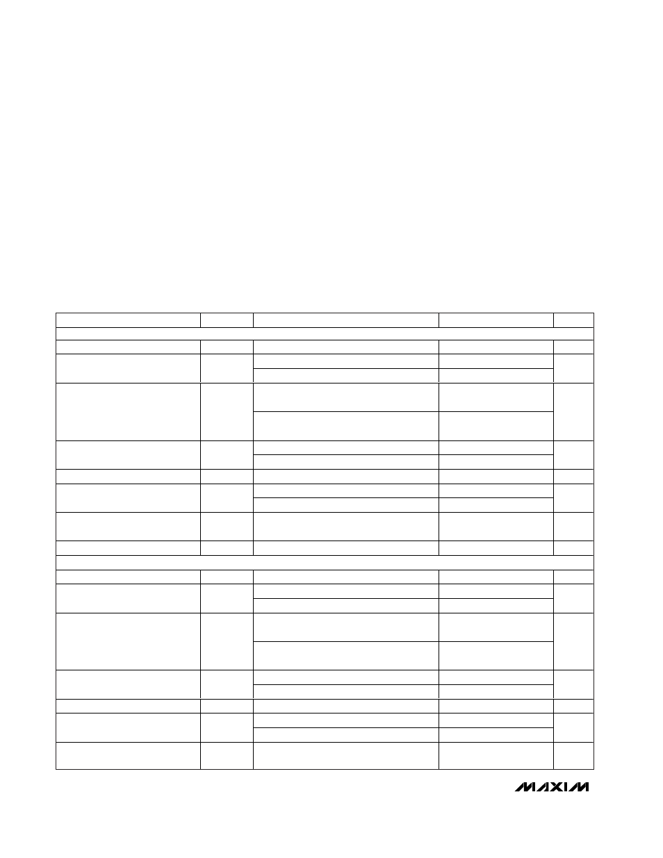
ABSOLUTE MAXIMUM RATINGS
ELECTRICAL CHARACTERISTICS
(V
DD
= +1.8V to +5.5V, OUT unloaded, T
A
= T
MIN
to T
MAX
, unless otherwise noted. Typical values are at T
A
= +25°C.)
Stresses beyond those listed under “Absolute Maximum Ratings” may cause permanent damage to the device. These are stress ratings only, and functional
operation of the device at these or any other conditions beyond those indicated in the operational sections of the specifications is not implied. Exposure to
absolute maximum rating conditions for extended periods may affect device reliability.
V
DD
to GND ..............................................................-0.3V to +6V
OUT to GND ...............................................-0.3V to (V
DD
+ 0.3V)
FB to GND ..................................................-0.3V to (V
DD
+ 0.3V)
SCLK, DIN,
CS to GND ..............................-0.3V to (V
DD
+ 0.3V)
REFIN, REFOUT to GND ............................-0.3V to (V
DD
+ 0.3V)
Continuous Power Dissipation (T
A
= +70°C)
Thin QFN (derate 16.9mW/°C above +70°C).............1349mW
Operating Temperature Range ...........................-40°C to +85°C
Storage Temperature Range .............................-65°C to +150°C
Junction Temperature ..................................................... +150°C
Lead Temperature (soldering, 10s) .................................+300°C
PARAMETER
SYMBOL
CONDITIONS
MIN
TYP
MAX
UNITS
STATIC ACCURACY (MAX5510 EXTERNAL REFERENCE)
Resolution
N
8
Bits
V
DD
= 5V, V
REF
= 4.096V
±0.25
±1
Integral Nonlinearity (Note 1)
INL
V
DD
= 1.8V, V
REF
= 1.024V
±0.25
±1
LSB
Guaranteed monotonic,
V
DD
= 5V, V
REF
= 4.096V
±0.2
±1
Differential Nonlinearity (Note 1)
DNL
Guaranteed monotonic,
V
DD
= 1.8V, V
REF
= 1.024V
±0.2
±1
LSB
V
DD
= 5V, V
REF
= 4.096V
±1
±20
Offset Error (Note 2)
V
OS
V
DD
= 1.8V, V
REF
= 1.024V
±1
±20
mV
Offset-Error Temperature Drift
±2
µV/°C
V
DD
= 5V, V
REF
= 4.096V
±0.5
±1
Gain Error (Note 3)
GE
V
DD
= 1.8V, V
REF
= 1.024V
±0.5
±1
LSB
Gain-Error Temperature
Coefficient
±4
ppm/°C
Power-Supply Rejection Ratio
PSRR
1.8V ≤ V
DD
≤ 5.5V
85
dB
STATIC ACCURACY (MAX5511 INTERNAL REFERENCE)
Resolution
N
8
Bits
V
DD
= 5V, V
REF
= 3.9V
±0.25
±1
Integral Nonlinearity (Note 1)
INL
V
DD
= 1.8V, V
REF
= 1.2V
±0.25
±1
LSB
Guaranteed monotonic,
V
DD
= 5V, V
REF
= 3.9V
±0.2
±1
Differential Nonlinearity (Note 1)
DNL
Guaranteed monotonic,
V
DD
= 1.8V, V
REF
= 1.2V
±0.2
±1
LSB
V
DD
= 5V, V
REF
= 3.9V
±1
±20
Offset Error (Note 2)
V
OS
V
DD
= 1.8V, V
REF
= 1.2V
±1
±20
mV
Offset-Error Temperature Drift
±2
µV/°C
V
DD
= 5V, V
REF
= 3.9V
±0.5
±1
Gain Error (Note 3)
GE
V
DD
= 1.8V, V
REF
= 1.2V
±0.5
±1
LSB
Gain-Error Temperature
Coefficient
±4
ppm/°C