Rainbow Electronics MAX19507 User Manual
Page 2
MAX19507
Dual-Channel, 8-Bit, 130Msps ADC
2
_______________________________________________________________________________________
ABSOLUTE MAXIMUM RATINGS
ELECTRICAL CHARACTERISTICS
(V
AVDD
= V
OVDD
= 1.8V, internal reference, differential clock, V
CLK
= 1.5V
P-P
, f
CLK
= 130MHz, A
IN
= -0.5dBFS, data output termina-
tion = 50Ω, T
A
= -40°C to +85°C, unless otherwise noted. Typical values are at T
A
= +25°C.) (Note 1)
Stresses beyond those listed under “Absolute Maximum Ratings” may cause permanent damage to the device. These are stress ratings only, and functional
operation of the device at these or any other conditions beyond those indicated in the operational sections of the specifications is not implied. Exposure to
absolute maximum rating conditions for extended periods may affect device reliability.
OVDD, AVDD to GND............................................-0.3V to +3.6V
CMA, CMB, REFIO, INA+, INA-, INB+,
INB- to GND ......................................................-0.3V to +2.1V
CLK+, CLK-, SYNC, SPEN, CS, SCLK, SDIN
to GND ..........-0.3V to the lower of (V
AVDD
+ 0.3V) and +3.6V
DCLKA, DCLKB, D7A–D0A, D7B–D0B, DORA, DORB
to GND ..........-0.3V to the lower of (V
OVDD
+ 0.3V) and +3.6V
Continuous Power Dissipation (T
A
= +70°C)
48-Pin Thin QFN, 7mm x 7mm x 0.8mm (derate 40mW/°C
above +70°C).............................................................3200mW
Operating Temperature Range ...........................-40°C to +85°C
Junction Temperature ......................................................+150°C
Storage Temperature Range .............................-65°C to +150°C
Lead Temperature (soldering, 10s) .................................+300°C
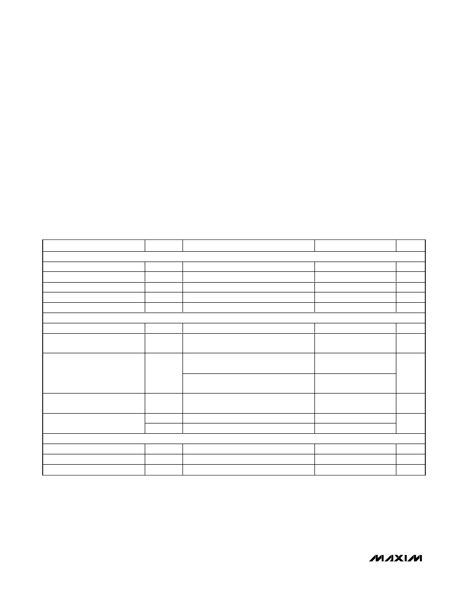
PARAMETER
SYMBOL
CONDITIONS
MIN
TYP
MAX
UNITS
DC ACCURACY
Resolution
8
Bits
Integral Nonlinearity
INL
f
IN
= 3MHz
-0.3
±0.1
+0.3
LSB
Differential Nonlinearity
DNL
f
IN
= 3MHz
-0.3
±0.1
+0.3
LSB
Offset Error
OE
Internal reference
-0.4
±0.1
+0.4
%FS
Gain Error
GE
External reference = 1.25V
-1.5
±0.3
+1.5
%FS
ANALOG INPUTS (INA+, INA-, INB+, INB-) (Figure 3)
Differential Input-Voltage Range
V
DIFF
Differential or single-ended inputs
1.5
V
P-P
Common-Mode Input-Voltage
Range
V
CM
(Note 2)
0.4
1.4
V
Fixed resistance, common mode, and
differential mode
> 100
Input Resistance
R
IN
Differential input resistance, common mode
connected to inputs
4
k
Ω
Input Current
I
IN
Switched capacitance common-mode input
current, each input
74
µA
C
PAR
Fixed capacitance to ground, each input
0.7
Input Capacitance
C
SAMPLE
Switched capacitance, each input
1.2
pF
CONVERSION RATE
Maximum Clock Frequency
f
CLK
130
MHz
Minimum Clock Frequency
f
CLK
65
MHz
Data Latency
Figures 9, 10
9
Cycles