Table1. parallel-interface pin functionality – Rainbow Electronics MAX19507 User Manual
Page 15
MAX19507
Dual-Channel, 8-Bit, 130Msps ADC
______________________________________________________________________________________
15
Reference Input/Output (REFIO)
REFIO adjusts the reference potential, which, in turn,
adjusts the full-scale range of the ADC. Figure 4 shows
a simplified schematic of the reference system. An
internal bandgap voltage generator provides an internal
reference voltage. The bandgap potential is buffered
and applied to REFIO through a 10kΩ resistor. Bypass
REFIO with a 0.1µF capacitor to AGND. The bandgap
voltage is applied to a scaling and level-shift circuit,
which creates internal reference potentials that estab-
lish the full-scale range of the ADC. Apply an external
voltage on REFIO to trim the ADC full scale. The allow-
able adjustment range is +5/-15%. The REFIO-to-ADC
gain transfer function is:
V
FS
= 1.5 x [V
REFIO
/1.25] Volts
Programming and Interface
There are two ways to control the MAX19507 operating
modes. Full feature selection is available using the SPI
interface, while the parallel interface offers a limited set
of commonly used features. The programming mode is
selected using the SPEN input. Drive SPEN low for SPI
interface; drive SPEN high for parallel interface.
Parallel Interface
The parallel interface offers a pin-programmable inter-
face with a limited feature set. Connect SPEN to AVDD
to enable the parallel interface. See Table 1 for pin
functionality; see Figure 5 for a simplified parallel-inter-
face input schematic.
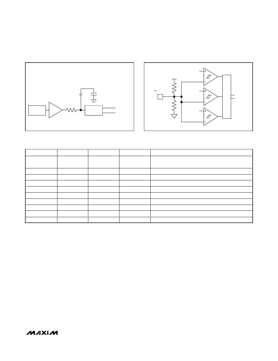
BANDGAP
REFERENCE
BUFFER
1.250V
REFIO
INTERNAL GAIN—BYPASS REFIO
EXTERNAL GAIN CONTROL—DRIVE REFIO
SCALE AND
LEVEL SHIFT
INTERNAL REFERENCE
(CONTROLS ADC GAIN)
10kΩ
0.1µF
EXTERNAL BYPASS
Figure 4. Simplified Reference Schematic
36kΩ
156kΩ
CS
SCLK
SDIN
AVDD
29/32 AVDD
DECODER
TO
CONTROL
LOGIC
23/32 AVDD
3/32 AVDD
Figure 5. Simplified Parallel-Interface Input Schematic
SPEN
SDIN/FORMAT
SCLK/DIV
CS/OUTSEL
DESCRIPTION
0
SDIN
SCLK
CS
SPI interface active. Features are programmed through the
serial port (see the Serial Programming Interface section).
1
0
X
X
Two’s complement
1
AVDD
X
X
Offset binary
1
Unconnected
X
X
Gray code
1
X
0
X
Clock divide-by-1
1
X
AVDD
X
Clock divide-by-2
1
X
Unconnected
X
Clock divide-by-4
1
X
X
0
CMOS (dual bus)
1
X
X
AVDD
MUX CMOS (channel A data bus)
1
X
X
Unconnected
MUX CMOS (channel B data bus)
Table1. Parallel-Interface Pin Functionality
X = Don’t care.