Electrical characteristics (continued) – Rainbow Electronics MAX5890 User Manual
Page 3
MAX5890
14-Bit, 600Msps, High-Dynamic-Performance
DAC with LVDS Inputs
_______________________________________________________________________________________
3
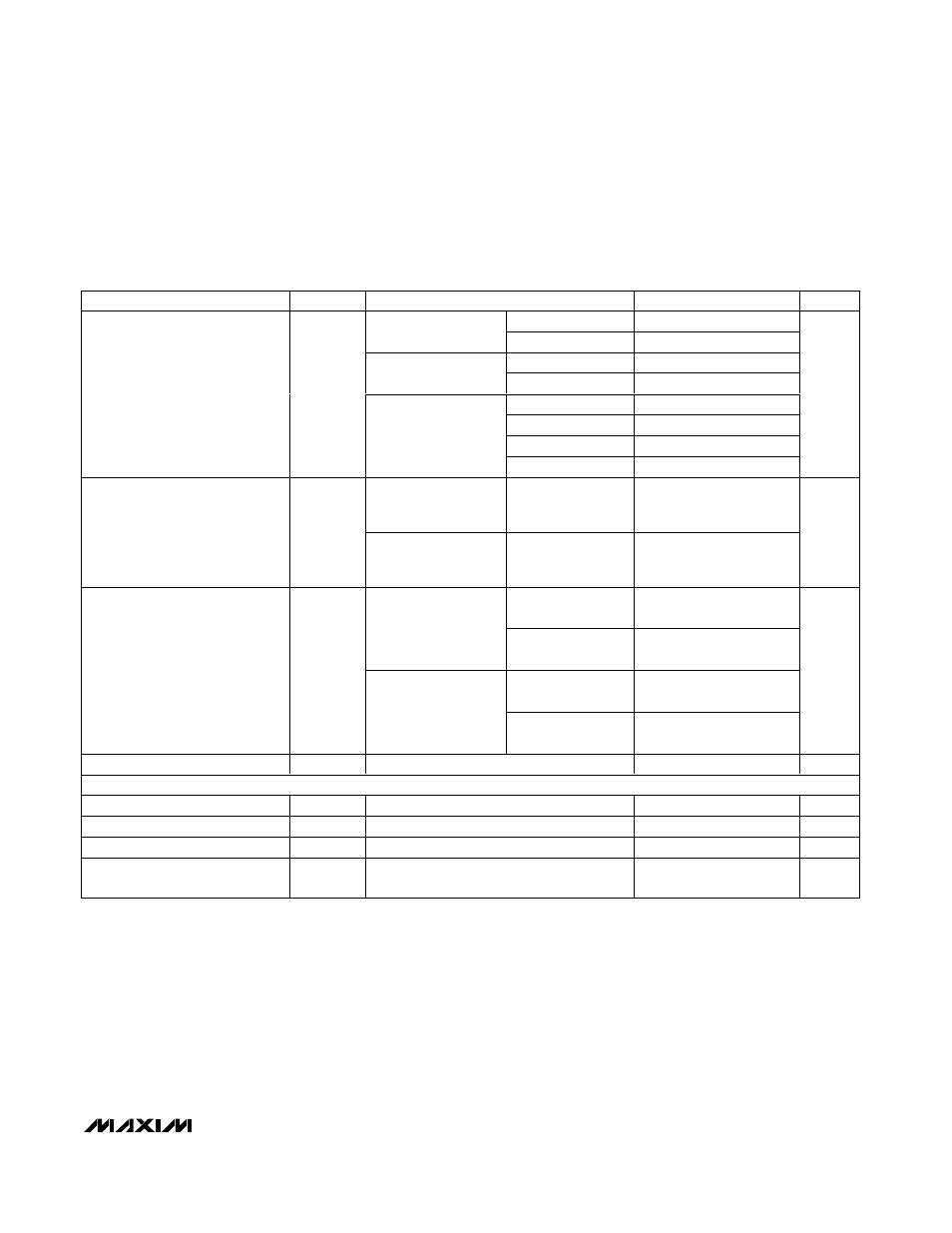
ELECTRICAL CHARACTERISTICS (continued)
(AV
DD3.3
= DV
DD3.3
= AV
CLK
= +3.3V, AV
DD1.8
= DV
DD1.8
= +1.8V, external reference V
REFIO
= +1.2V, output load 50
Ω double-ter-
minated, transformer-coupled output, I
OUT
= 20mA, T
A
= -40°C to +85°C, unless otherwise noted. Specifications at T
A
≥ +25°C are
guaranteed by production testing. Specifications at T
A
< +25°C are guaranteed by design and characterization. Typical values are at
T
A
= +25°C.)
PARAMETER
SYMBOL
CONDITIONS
MIN
TYP
MAX
UNITS
f
OUT
= 16MHz
86
f
CLK
= 200MHz,
0dBFS
f
OUT
= 30MHz
86
f
OUT
= 16MHz
78
f
CLK
= 200MHz,
-12dBFS
f
OUT
= 30MHz
78
f
OUT
= 16MHz
77
84
f
OUT
= 30MHz
80
f
OUT
= 130MHz
68
Spurious-Free
Dynamic Range to
Nyquist
SFDR
f
CLK
= 500MHz,
0dBFS
f
OUT
= 200MHz
63
dBc
f
CLK
= 500MHz
f
OUT1
= 29MHz,
f
OUT2
= 30MHz,
-6.5dBFS per tone
-93
Two-Tone IMD
TTIMD
f
CLK
= 500MHz
f
OUT1
= 129MHz,
f
OUT2
= 130MHz,
-6.5dBFS per tone
-76
dBc
f
CLK
= 491.52MHz,
f
OUT
= 30.72MHz
82
WCDMA single
carrier
f
CLK
= 491.52MHz,
f
OUT
= 122.88MHz
73
f
CLK
= 491.52MHz,
f
OUT
= 30.72MHz
74
Adjacent Channel
Leakage Power Ratio
ACLR
WCDMA four carriers
f
CLK
= 491.52MHz,
f
OUT
= 122.88MHz
67
dB
Output Bandwidth
BW
-1dB
(Note 2)
1000
MHz
REFERENCE
Internal Reference Voltage Range
V
REFIO
1.14
1.2
1.26
V
Reference Input Voltage Range
V
REFIOCR
Using external reference
0.10
1.2
1.32
V
Reference Input Resistance
R
REFIO
10
k
Ω
Reference Voltage Temperature
Drift
TCO
REF
±50
ppm/
°C