Max5890 – Rainbow Electronics MAX5890 User Manual
Page 12

MAX5890
Grounding, Bypassing, and Power-Supply
Considerations
Grounding and power-supply decoupling strongly influ-
ence the MAX5890 performance. Unwanted digital
crosstalk coupling through the input, reference, power
supply, and ground connections affects dynamic per-
formance. High-speed, high-frequency applications
require closely followed proper grounding and power-
supply decoupling. These techniques reduce EMI and
internal crosstalk that can significantly affect the
MAX5890 dynamic performance.
Use a multilayer printed circuit (PC) board with sepa-
rate ground and power-supply planes. Run high-speed
signals on lines directly above the ground plane. Keep
digital signals as far away from sensitive analog inputs
and outputs, reference input sense lines, common-
mode inputs, and clock inputs as practical. Use a sym-
metric design of clock input and the analog output lines
to minimize 2nd-order harmonic-distortion components,
thus optimizing the DAC’s dynamic performance. Keep
digital signal paths short and run lengths matched to
avoid propagation delay and data skew mismatches.
The MAX5890 requires five separate power-supply
inputs for analog (AV
DD1.8
and AV
DD3.3
), digital
(DV
DD1.8
and DV
DD3.3
), and clock (AV
CLK
) circuitry.
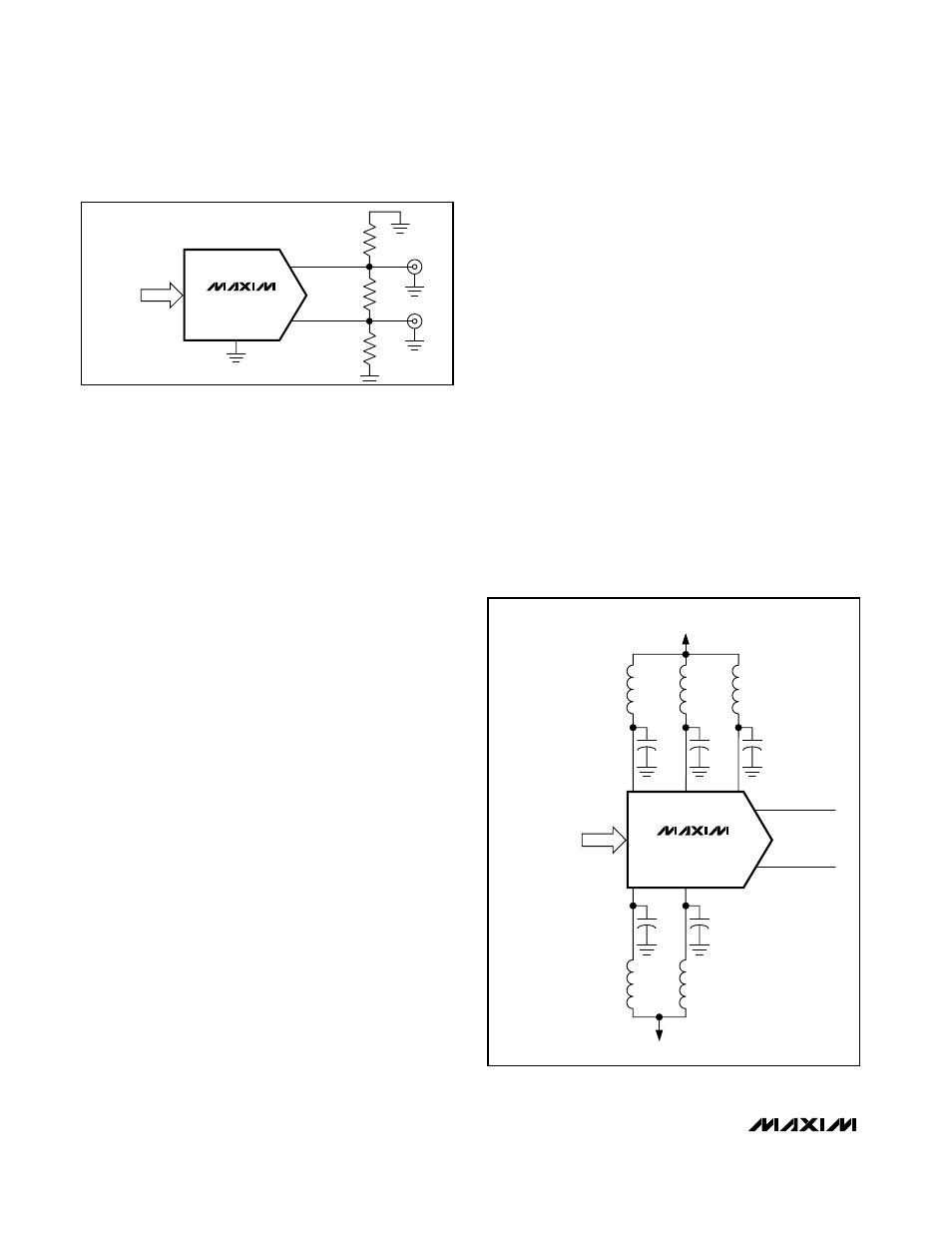
Decouple each AV
DD3.3
, AV
DD1.8
, AV
CLK
, DV
DD3.3
, and
DV
DD1.8
input with a separate 0.1µF capacitor as close
to the device as possible with the shortest possible con-
nection to the respective ground plane (Figure 7).
Connect all of the 3.3V supplies together at one point
with ferrite beads to minimize supply noise coupling.
Decouple all five power-supply voltages at the point they
enter the PC board with tantalum or electrolytic capaci-
tors. Ferrite beads with additional decoupling capacitors
forming a pi network can also improve performance.
Similarly, connect all 1.8V supplies together at one point
with ferrite beads.
The analog and digital power-supply inputs AV
DD3.3
,
AV
CLK
, and DV
DD3.3
allow a +3.135V to +3.465V sup-
ply voltage range. The analog and digital power-supply
inputs AV
DD1.8
and DV
DD1.8
allow a +1.71V to +1.89V
supply voltage range.
The MAX5890 is packaged in a 68-pin QFN-EP pack-
age with exposed paddle, providing optimized DAC AC
performance. The exposed pad must be soldered to
the ground plane of the PC board. Thermal efficiency is
not the key factor, since the MAX5890 features low-
power operation. The exposed pad ensures a solid
ground connection between the DAC and the PC
board’s ground layer.
The data converter die attaches to an EP lead frame
with the back of this frame exposed at the package
bottom surface, facing the PC board side of the pack-
age. This allows for a solid attachment of the package
to the PC board with standard infrared (IR) reflow sol-
dering techniques. A specially created land pattern on
the PC board, matching the size of the EP (6mm x
6mm), ensures the proper attachment and grounding of
the DAC. Place vias into the land area and implement
14-Bit, 600Msps, High-Dynamic-Performance
DAC with LVDS Inputs
12
______________________________________________________________________________________
MAX5890
OUTP
OUTN
AGND
25
Ω
50
Ω
25
Ω
OUTP
OUTN
D0–D13
LVDS
DATA INPUTS
Figure 6. Differential Output Configuration
MAX5890
OUTP
AV
DD3.3
AV
DD1.8
DV
DD3.3
DV
DD1.8
AV
CLK
OUTN
0.1
µF
3.3V VOLTAGE SUPPLY
0.1
µF
0.1
µF
0.1
µF
1.8V VOLTAGE SUPPLY
0.1
µF
BYPASSING—DAC LEVEL
*FERRITE BEADS
D0–D13
LVDS
DATA INPUTS
*
*
*
*
*
Figure 7. Recommended Power-Supply Decoupling and
Bypassing Circuitry
