Max5890, Clock inputs (clkp, clkn), Data-timing relationship – Rainbow Electronics MAX5890 User Manual
Page 10: Lvds data inputs, Power-down operation (pd)

MAX5890
Clock Inputs (CLKP, CLKN)
To achieve the best possible jitter performance, the
MAX5890 features flexible differential clock inputs
(CLKP, CLKN) that operate from a separate clock
power supply (AV
CLK
). Drive the differential clock
inputs from a single-ended or a differential clock
source. For highest dynamic performance, differential
clock source is required. For single-ended operation,
drive CLKP and bypass CLKN to CGND.
CLKP and CLKN are internally biased at AV
CLK
/ 2,
allowing the AC-coupling of clock sources directly to
the device without external resistors to define the DC
level. The input resistance from CLKP and CLKN to
ground is approximately 5k
Ω.
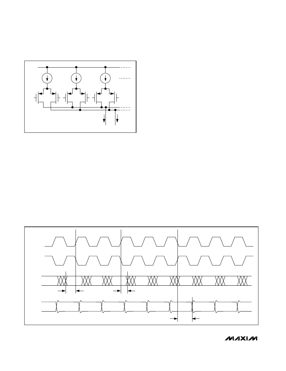
Data-Timing Relationship
Figure 3 shows the timing relationship between digital
LVDS data, clock, and output signals. The MAX5890
features a 2ns hold, a -1.2ns setup, and a 2.5ns propa-
gation delay time. There is a 5.5 clock-cycle latency
between data write operation and the corresponding
analog output transition.
LVDS Data Inputs
The MAX5890 has 14 pairs of LVDS data inputs (offset
binary format) and can accept data rates up to
600MWps. Each differential input pair is terminated with
an internal 110
Ω resistor. The common-mode input
resistance is 3.2k
Ω.
Power-Down Operation (PD)
The MAX5890 features a power-down mode that
reduces the DAC’s power consumption. Set PD high to
power down the MAX5890. Set PD low or leave uncon-
nected for normal operation.
When powered down, the MAX5890 overall power con-
sumption is reduced to less than 13µW. The MAX5890
requires 350µs to wake up from power-down and enter
a fully operational state if the external reference is
used. If the internal reference is used, the power-down
recovery time is 10ms. The PD internal pulldown circuit
sets the MAX5890 in normal mode when PD is left
unconnected.
14-Bit, 600Msps, High-Dynamic-Performance
DAC with LVDS Inputs
10
______________________________________________________________________________________
I
OUT
I
OUT
OUTN OUTP
CURRENT
SOURCES
CURRENT
SWITCHES
AV
DD3.3
Figure 2. Simplified Analog Output Structure
D0–D13
t
SETUP
t
HOLD
D
N
CLKP
CLKN
D
N + 2
D
N + 4
D
N + 6
IOUTP
IOUTN
t
PD
D
N + 1
D
N + 3
D
N + 5
D
N + 7
OUT
N - 2
OUT
N - 3
OUT
N - 4
OUT
N - 5
OUT
N - 6
OUT
N - 7
OUT
N-1
OUT
N
Figure 3. Timing Relationship Between Clock, Input Data, and Analog Output
