Detailed description, Table 1. i, And r – Rainbow Electronics MAX5889 User Manual
Page 9

Detailed Description
Architecture
The MAX5889 high-performance, 12-bit, current-steer-
ing DAC (see the Functional Diagram) operates with
DAC update rates up to 600Msps. The current-steering
array generates differential full-scale currents in the
2mA to 20mA range. An internal current-switching net-
work, in combination with external 50
Ω termination
resistors, converts the differential output currents into a
differential output voltage with a 0.1V to 1V peak-to-
peak output voltage range. The analog outputs have a
-1.0V to +1.1V voltage compliance. For applications
requiring high dynamic performance, use the differen-
tial output configuration and limit the output voltage
swing to ±0.5V at each output. An integrated +1.2V
bandgap reference, control amplifier, and user-selec-
table external resistor determine the data converter’s
full-scale output range.
Reference Architecture and Operation
The MAX5889 operates with the internal +1.2V
bandgap reference or an external reference voltage
source. REFIO serves as the input for an external, low-
impedance reference source or as a reference output
when the DAC operates in internal reference mode. For
stable operation with the internal reference, bypass
REFIO to AGND with a 0.1µF capacitor. The REFIO out-
put resistance is 10k
Ω. Buffer REFIO with a high-input-
impedance amplifier when using it as a reference
source for external circuitry.
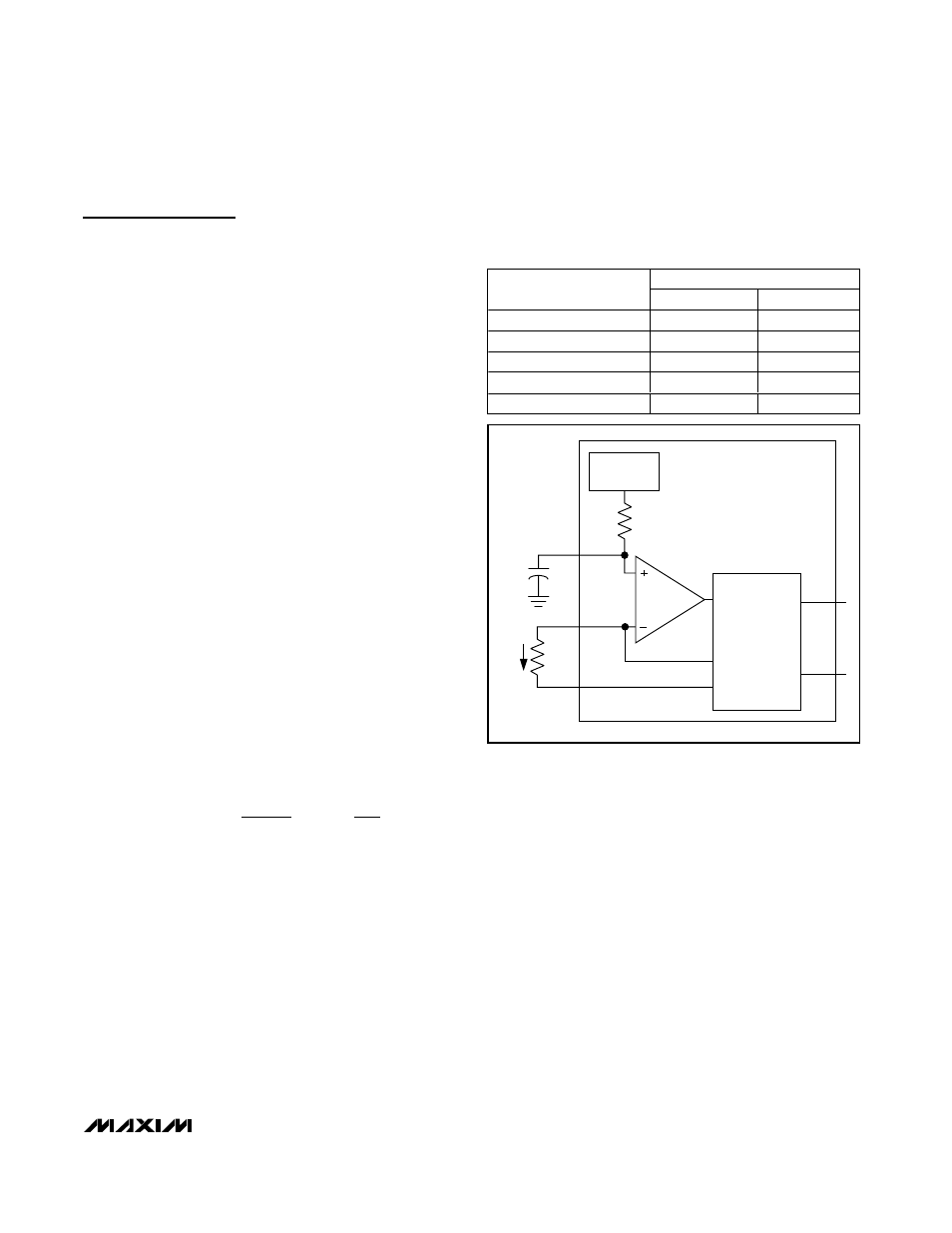
The MAX5889’s reference circuit (Figure 1) employs a
control amplifier to regulate the full-scale current,
I
OUTFS
, for the differential current outputs of the DAC.
Calculate the output current as follows:
where I
OUTFS
is the full-scale output current of the
DAC. R
SET
(located between FSADJ and DACREF)
determines the amplifier’s full-scale output current for
the DAC. See Table 1 for a matrix of different I
OUTFS
and R
SET
selections.
Analog Outputs (OUTP, OUTN)
The complementary current outputs (OUTP, OUTN) can
be connected in a single-ended or differential configu-
ration. A load resistor converts these two output cur-
rents into complementary single-ended output
voltages. A transformer or a differential amplifier con-
verts the differential voltage existing between OUTP
and OUTN to a single-ended voltage. When not using a
transformer, terminate each output with a 25
Ω resistor
to ground and a 50
Ω resistor between the outputs.
To generate a single-ended output, select OUTP as the
output and connect OUTN to AGND. Figure 2 shows a
simplified diagram of the internal output structure of the
MAX5889.
I
V
R
OUTFS
REFIO
SET
=
Ч
Ч
−
32
1
1
2
12
MAX5889
12-Bit, 600Msps, High-Dynamic-Performance
DAC with LVDS Inputs
_______________________________________________________________________________________
9
R
SET
(k
Ω)
FULL-SCALE CURRENT
I
OUTFS
(mA)
CALCULATED
1% EIA STD
2
19.2
19.1
5
7.68
7.5
10
3.84
3.83
15
2.56
2.55
20
1.92
1.91
Table 1. I
OUTFS
and R
SET
Selection Matrix
Based on a Typical +1.200V Reference
Voltage
OUTP
OUTN
+1.2V
REFERENCE
CURRENT-SOURCE
ARRAY DAC
REFIO
FSADJ
R
SET
I
REF
10k
Ω
DACREF
0.1
µF
I
REF
= V
REFIO
/ R
SET
Figure 1. Reference Architecture, Internal Reference
Configuration
