Electrical characteristics (continued) – Rainbow Electronics MAX5889 User Manual
Page 4

MAX5889
12-Bit, 600Msps, High-Dynamic-Performance
DAC with LVDS Inputs
4
_______________________________________________________________________________________
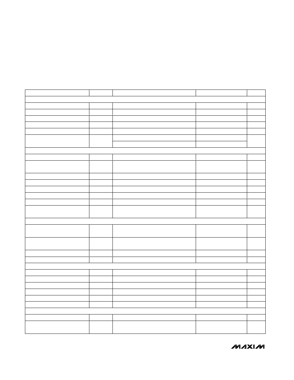
ELECTRICAL CHARACTERISTICS (continued)
(AV
DD3.3
= DV
DD3.3
= AV
CLK
= +3.3V, AV
DD1.8
= DV
DD1.8
= +1.8V, external reference V
REFIO
= +1.2V, output load 50
Ω double-ter-
minated, transformer-coupled output, I
OUT
= 20mA, T
A
= -40°C to +85°C, unless otherwise noted. Specifications at T
A
≥ +25°C are
guaranteed by production testing. Specifications at T
A
< +25°C are guaranteed by design and characterization. Typical values are at
T
A
= +25°C.)
PARAMETER
SYMBOL
CONDITIONS
MIN
TYP
MAX
UNITS
ANALOG OUTPUT TIMING (Figure 3)
Output Fall Time
t
FALL
90% to 10% (Note 3)
0.4
ns
Output Rise Time
t
RISE
10% to 90% (Note 3)
0.4
ns
Output Propagation Delay
t
PD
Reference to data latency (Note 3)
2.5
ns
Output Settling Time
To 0.025% of the final value (Note 3)
11
ns
Glitch Impulse
Measured differentially
1
pV
•
s
I
OUT
= 2mA
30
Output Noise
N
OUT
I
OUT
= 20mA
30
pA/
√Hz
TIMING CHARACTERISTICS
Input Data Rate
600
MWps
Data Latency
5.5
Clock
cycles
Data to Clock Setup Time
t
SETUP
Referenced to rising edge of clock (Note 4)
-1.2
ns
Data to Clock Hold Time
t
HOLD
Referenced to rising edge of clock (Note 4)
2
ns
Clock Frequency
f
CLK
CLKP, CLKN
600
MHz
Minimum Clock Pulse-Width High
t
CH
CLKP, CLKN
0.6
ns
Minimum Clock Pulse-Width Low
t
CL
CLKP, CLKN
0.6
ns
Turn-On Time
t
SHDN
External reference, PD falling edge to
output settle within 1%
350
µs
CMOS LOGIC INPUT (PD)
Input Logic High
V
IH
0.7 x
DV
DD3.3
V
Input Logic Low
V
IL
0.3 x
DV
DD3.3
V
Input Current
I
IN
-10
±1.8
+10
µA
Input Capacitance
C
IN
3
pF
LVDS INPUTS
Differential Input High
V
IHLVDS
+100
mV
Differential Input Low
V
ILLVDS
-100
mV
Common-Mode Voltage Range
V
ICMLVDS
1.125
1.375
V
Differential Input Resistance
R
IDLVDS
110
Ω
Common-Mode Input Resistance
R
ICMLVDS
3.2
k
Ω
Input Capacitance
C
INLVDS
3
pF
DIFFERENTIAL CLOCK INPUTS (CLKP, CLKN)
Clock Common-Mode Voltage
CLKP and CLKN are internally biased
AV
CLK
/ 2
V
Minimum Differential Input
Voltage Swing
0.5
V
P-P
