Applications information – Rainbow Electronics MAX5889 User Manual
Page 11

Applications Information
Clock Interface
To achieve the best possible jitter performance, the
MAX5889 features flexible differential clock inputs
(CLKP, CLKN) that operate from a separate clock
power supply (AV
CLK
). Use a low-jitter clock to reduce
the DAC’s phase noise and wideband noise. To
achieve the best DAC dynamic performance, the
CLKP/CLKN input source must be designed carefully.
The differential clock (CLKN and CLKP) input can be
driven from a single-ended or a differential clock
source. Use differential clock drive to achieve the best
dynamic performance from the DAC. For single-ended
operation, drive CLKP with a low-noise source and
bypass CLKN to CGND with a 0.1µF capacitor.
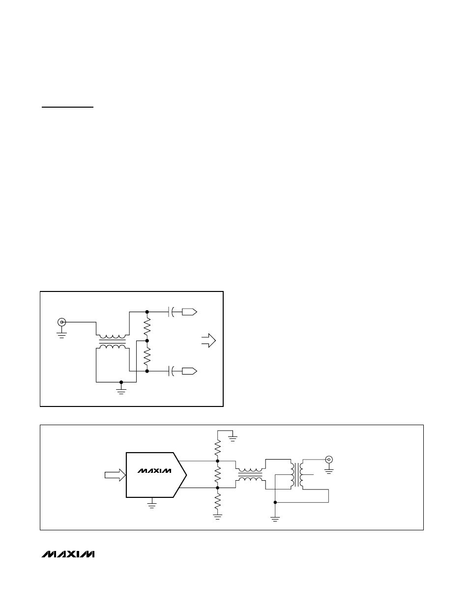
Figure 4 shows a convenient and quick way of applying
a differential signal created from a single-ended source
using a wideband transformer. Alternatively, drive
CLKP/CLKN from a CMOS-compatible clock source.
Use sine wave or AC-coupled differential ECL/PECL
drive for best dynamic performance.
Differential Output Coupling Using a
Wideband RF Transformer
Use a pair of transformers (Figure 5) or a differential
amplifier configuration to convert the differential voltage
existing between OUTP and OUTN to a single-ended
voltage. Optimize the dynamic performance by using a
differential transformer-coupled output and limit the out-
put power to <0dBm full scale. To achieve the best
dynamic performance, use the differential transformer
configuration. Terminate the DAC as shown in Figure 5,
and use 50
Ω termination at the transformer single-
ended output. This provides double 50
Ω termination for
the DAC output network. With the double-terminated
output and 20mA full-scale current, the DAC produces a
full-scale signal level of approximately -2dBm. Pay close
attention to the transformer core saturation characteris-
tics when selecting a transformer for the MAX5889.
Transformer core saturation can introduce strong 2nd-
order harmonic distortion especially at low output fre-
quencies and high signal amplitudes. For best results,
connect the center tap of the transformer to ground.
When not using a transformer, terminate each DAC out-
put to ground with a 25
Ω resistor. Additionally, place a
50
Ω resistor between the outputs (Figure 6).
For a single-ended unipolar output, select OUTP as the
output and connect OUTN to AGND. Operating the
MAX5889 single-ended is not recommended because
it degrades the dynamic performance.
The distortion performance of the DAC depends on the
load impedance. The MAX5889 is optimized for 50
Ω
differential double termination. Using higher termination
impedance degrades distortion performance and
increases output noise voltage.
MAX5889
12-Bit, 600Msps, High-Dynamic-Performance
DAC with LVDS Inputs
______________________________________________________________________________________
11
WIDEBAND RF TRANSFORMER
PERFORMS SINGLE-ENDED-TO-
DIFFERENTIAL CONVERSION
SINGLE-ENDED
CLOCK SOURCE
AGND
1:1
25
Ω
25
Ω
CLKP
CLKN
TO DAC
0.1
µF
0.1
µF
Figure 4. Differential Clock-Signal Generation
MAX5889
OUTP
OUTN
WIDEBAND RF TRANSFORMER T2 PERFORMS THE
DIFFERENTIAL-TO-SINGLE-ENDED CONVERSION
T1, 1:1
T2, 1:1
AGND
50
Ω
100
Ω
50
Ω
V
OUT
, SINGLE-ENDED
D0–D11
LVDS
DATA INPUTS
Figure 5. Differential-to-Single-Ended Conversion Using a Wideband RF Transformer
