3 packages characteristics, Atvaultic200 – Rainbow Electronics ATVaultIC200 User Manual
Page 18
18
TPR0460AX–SMS–02/10
ATVaultIC200
3.6.3
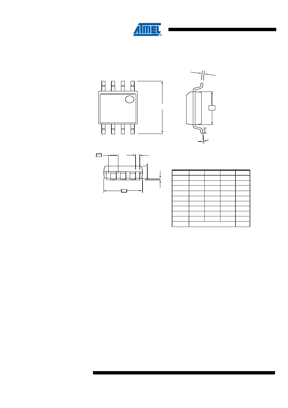
Packages characteristics
Figure 3-8.
SOIC-8 package characteristics
COMMON DIMENSIONS
(Unit of Measure = mm)
SYMBOL
MIN
NOM
MAX
NOTE
Notes: 1. This drawing is for general information only; refer to EIAJ Drawing EDR-7320 for additional information.
2. Mismatch of the upper and lower dies and resin burrs are not included.
3. It is recommended that upper and lower cavities be equal. If they are different, the larger dimension shall be regarded.
4. Determines the true geometric position.
5. Values b and C apply to pb/Sn solder plated terminal.
The standard thickness of the solder layer shall be 0.010 +0.010/-0.005 mm.
A
1.70
2.16
A1
0.05
0.25
b
0.35
0.48
5
C
0.15
0.35
5
D
5.13
5.35
E1
5.18
5.40
2, 3
E
7.70
8.26
L
0.51
0.85
?
0˚
8˚
e
1.27 BSC
4
End View
Side View
e
b
A
A1
D
E
N
1
C
E1
?
L
Top View