Electrical characteristics, Absolute maximum ratings – Rainbow Electronics MAX16074 User Manual
Page 2
2 ______________________________________________________________________________________
MAX16072/MAX16073/MAX16074
µP Supervisory Circuits in
4-Bump (1mm x 1mm) Chip-Scale Package
Stresses beyond those listed under “Absolute Maximum Ratings” may cause permanent damage to the device. These are stress ratings only, and functional
operation of the device at these or any other conditions beyond those indicated in the operational sections of the specifications is not implied. Exposure to absolute
maximum rating conditions for extended periods may affect device reliability.
(Voltages referenced to GND.)
V
CC
, MR ..................................................................-0.3V to +6V
RESET, RESET Push-Pull ......................... -0.3V to (V
CC
+ 0.3V)
RESET Open-Drain ..................................................-0.3V to +6V
Output Current (all pins) ................................................. Q20mA
Continuous Power Dissipation (T
A
= +70NC)
4-Bump UCSP (derate 3mW/NC above +70NC) ..........239mW
Operating Temperature Range .......................... -40NC to +85NC
Storage Temperature Range ............................ -65NC to +150NC
Junction Temperature .....................................................+150NC
Soldering Temperature (reflow) ......................................+260NC
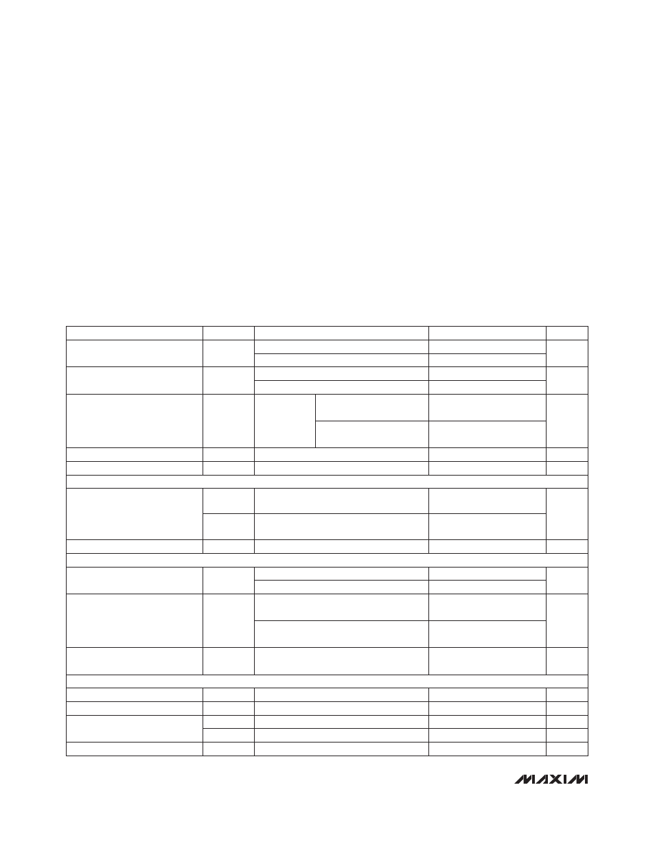
ELECTRICAL CHARACTERISTICS
(V
CC
= 1.5V to 2.75V, T
A
= -40NC to +85NC, unless otherwise noted. Typical values are at T
A
= +25NC and V
CC
= 3.6V.) (Note 1)
ABSOLUTE MAXIMUM RATINGS
PARAMETER
SYMBOL
CONDITIONS
MIN
TYP
MAX
UNITS
Operating Voltage Range
V
CC
T
A
= 0NC to +85NC
1.0
5.5
V
T
A
= -40NC to +85NC
1.2
5.5
Supply Current
I
CC
V
CC
= 1.8V for V
TH
P 1.66V
0.7
1.2
F
A
V
CC
= 3.6V, no load
1.0
1.5
Detector Threshold
V
TH
See Table 1
V
CC
falling, T
A
= +25NC
V
TH
-
1.5%
V
TH
V
TH
+
1.5%
V
V
CC
falling, T
A
= -40NC to
+85NC
V
TH
-
2.5%
V
TH
V
TH
+
2.5%
Detector Threshold Hysteresis
V
HYST
V
CC
rising, V
TH
P 1.66V (Note 2)
6.3
mV
Detector Threshold Tempco
D
V
TH
/NC
(Note 2)
40
ppm/NC
MR INPUT
MR Input High Voltage
V
IH
0.7 x
V
CC
V
V
IL
0.7 x
V
CC
MR Pullup Resistance
25
50
75
kI
RESET/RESET OUTPUT (Note 3)
Output-Voltage Low
V
OL
V
CC
R 1.2V, I
SINK
= 100FA
0.4
V
V
CC
R 1.65V, I
SINK
= 1mA
0.3
Output-Voltage High
V
OH
V
CC
R 1.65V, I
SOURCE
= 500FA
0.8 x
V
CC
V
V
CC
R 1.2V, I
SOURCE
= 50FA
0.8 x
V
CC
Open-Drain RESET Output
Leakage Current
RESET not asserted (Note 2)
0.1
F
A
TIMING
MR Minimum Pulse Width
t
MPW
(Note 2)
0.8
F
s
MR Glitch Rejection
t
EGR
(Note 2)
100
ns
MR to RESET/RESET
Propagation Delay
t
OFF
MR falling
1
2
F
s
t
ON
MR rising
200
400
ns
V
CC
to Reset Delay
t
DL
V
CC
= (V
TH
+ 100mV) to (V
TH
-100mV)
20
90
F
s