Absolute maximum ratings, Electrical characteristics – Rainbow Electronics MAX6616 User Manual
Page 2
MAX6615/MAX6616
Dual-Channel Temperature Monitors and
Fan-Speed Controllers with Thermistor Inputs
2
_______________________________________________________________________________________
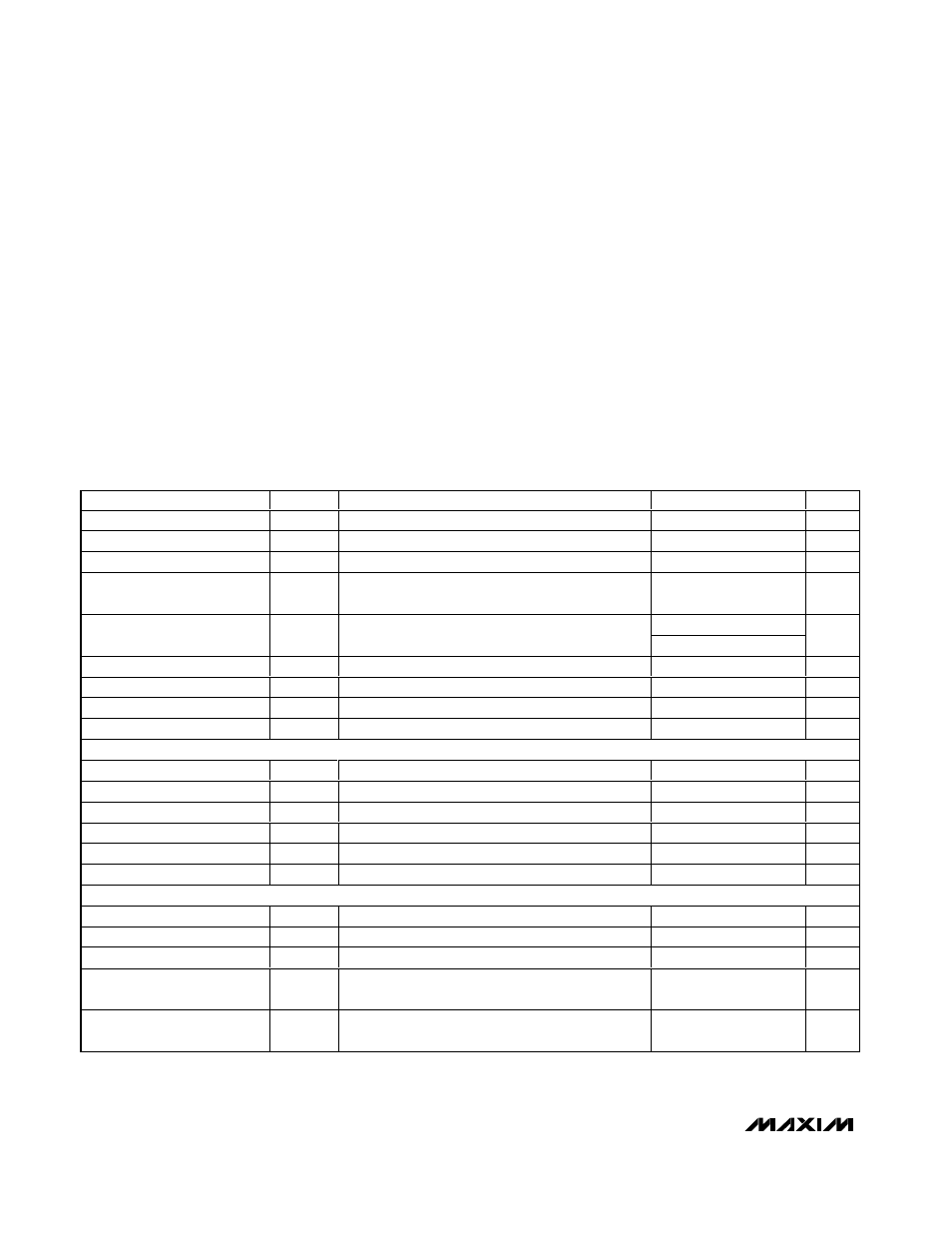
ABSOLUTE MAXIMUM RATINGS
Stresses beyond those listed under “Absolute Maximum Ratings” may cause permanent damage to the device. These are stress ratings only, and functional
operation of the device at these or any other conditions beyond those indicated in the operational sections of the specifications is not implied. Exposure to
absolute maximum rating conditions for extended periods may affect device reliability.
All Voltages Are Referenced to GND
Supply Voltage (V
CC
) ...............................................-0.3V to +6V
PWM_, TACH_, OT, FAN_FAIL ............................-0.3V to +13.5V
ADD0, ADD1, SDA, SCL ..........................................-0.3V to +6V
All Other Pins..............................................-0.3V to (V
CC
+ 0.3V)
SDA, OT, FAN_FAIL, PWM_, GPIO_ Current....................±50mA
TH_ Current ........................................................................±1mA
REF Current ......................................................................±20mA
Continuous Power Dissipation (T
A
= +70°C)
16-Pin QSOP (derated at 8.3mW/°C
above +70°C)............................................................666.7mW
24-Pin QSOP (derated at 9.5mW/°C
above +70°C)...........................................................761.9 mW
ESD Protection (all pins, Human Body Model) ....................±2kV
Operating Temperature Range .........................-40°C to +125°C
Junction Temperature ......................................................+150°C
Storage Temperature Range .............................-65°C to +150°C
Lead Temperature (soldering, 10s) .................................+300°C
ELECTRICAL CHARACTERISTICS
(V
CC
= +3.0V to +5.5V, T
A
= 0°C to +125°C, unless otherwise noted. Typical values are at V
CC
= +3.3V, T
A
= +25°C.)
PARAMETER
SYMBOL
CONDITIONS
MIN
TYP
MAX
UNITS
Operating Supply Voltage
V
CC
3.0
5.5
V
Standby Current
Interface inactive, ADC in idle state
10
µA
Operating Current
I
S
Interface inactive, ADC active
0.5
1
mA
External Temperature Error
V
CC
= +3.3V, 0.15V
≤ V
TH_
≤ +0.71V (excludes
thermistor errors, thermistor nonlinearity) (Note1)
±1
°C
V
CC
= +3.3V, 0°C
≤ T
A
≤ +85°C,
±2.5
Internal Temperature Error
V
CC
= +3.3V, 0°C
≤ T
A
≤ +125°C
±4
°C
Temperature Resolution
0.125
°C
Conversion Time
250
ms
Conversion Rate Timing Error
-20
+20
%
PWM Frequency Error
-20
+20
%
INPUT/OUTPUT
Output Low Voltage
V
OL
V
CC
= +3V, I
OUT
= 6mA
0.4
V
Output High Leakage Current
I
OH
1
µA
Logic Low Input Voltage
V
IL
0.8
V
Logic High Input Voltage
V
IH
2.1
V
Input Leakage Current
1
µA
Input Capacitance
C
IN
5
pF
SMBus TIMING (Figures 2, 3) (Note 2)
Serial Clock Frequency
f
SCLK
10
400
kHz
Clock Low Period
t
LOW
10% to 10%
4
µs
Clock High Period
t
HIGH
90% to 90%
4.7
µs
Bus Free Time Between STOP
and START Conditions
t
BUF
4.7
µs
SMBus START Condition
Setup Time
t
SU:STA
90% of SCL to 90% of SDA
4.7
µs