Table 2. slave address decoding (add0 and add1) – Rainbow Electronics MAX6616 User Manual
Page 11
GPIO Inputs/Outputs and
Preset (MAX6616)
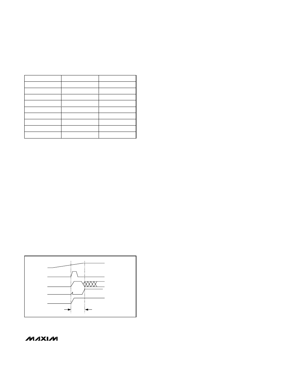
The MAX6616 has six GPIO ports. GPIO0 has a POR
control pin (PRESET). When PRESET is connected to
GND at POR, GPIO0 is configured as an output and is
low. When PRESET is connected to V
CC
at POR, GPIO0
is configured as an input. Since GPIO0 is a high-
impedance node in this state, it can be connected to a
pullup resistor and also serve as an output (high). The
rest of the GPIO ports, GPIO5–GPIO1, are configured
as high-impedance outputs after power-on, so they will
be in the high state if connected to pullup resistors. All
GPIOs are at their preset values within 1ms of power-
up. During power-up, GPIO1 and GPIO2 are low while
the remaining GPIOs go into high-impedance state.
Figure 8 shows the states of the GPIO lines during
power-up. After power has been applied to the
MAX6616, the GPIO functions can be changed through
the SMBus interface.
Register Descriptions
The MAX6615/MAX6616 contain 32/34 internal regis-
ters. These registers store temperature data, allow con-
trol of the PWM outputs, determine if the devices are
measuring from the internal die or the thermistor inputs,
and set the GPIO as inputs or outputs.
Temperature Registers (00h and 01h)
The temperature registers contain the results of temper-
ature measurements. The value of the MSB is 128°C and
the value of the LSB is 1°C. Temperature data for ther-
mistor channel 1 is in the temperature channel 1 register
(00h). Temperature data for thermistor channel 2 (01h)
or the local sensor (selectable by bit D2 in the configura-
tion byte) is in the temperature channel 2 register.
Configuration Byte (02h)
The configuration byte register controls timeout condi-
tions and various PWM signals. The POR state of the
configuration byte register is 18h. See Table 4 for con-
figuration byte definitions.
Channel 1 and Channel 2 O
OT
T Limits (03h and 04h)
Set channel 1 (03h) and channel 2 (04h) temperature
thresholds with these two registers. Once the temperature
is above the threshold, the OT output is asserted low (for
the temperature channels that are not masked). The POR
state of the channel 1 OT limit register is 6Eh, and the
POR state of the channel 2 OT limit register is 50h.
O
OT
T
Status (05h)
A 1 in D7 or D6 indicates that an OT fault has occurred
in the corresponding temperature channel. Only read-
ing its contents clears this register. Reading the con-
tents of the register also clears the OT output. If the
fault is still present on the next temperature measure-
ment cycle, the bits and the OT output are set again.
The POR state of the OT status register is 00h.
O
OT
T
Mask (06h)
Set bit D7 to 1 in the OT mask register to prevent the
OT output from asserting on faults in channel 1. Set bit
D6 to 1 to prevent the OT output from asserting on
faults in channel 2. The POR state of the OT mask reg-
ister is 00h.
PWM Start Duty Cycle (07h and 08h)
The PWM start duty-cycle register determines the PWM
duty cycle where the fan starts spinning. Bit D2 in the
configuration byte register (MIN DUTY CYCLE) deter-
mines the starting duty cycle. If the MIN DUTY CYCLE
bit is 1, the duty cycle is the value written to the fan-
start duty-cycle register at all temperatures below the
fan-start temperature. If the MIN DUTY CYCLE bit is
MAX6615/MAX6616
Dual-Channel Temperature Monitors and
Fan-Speed Controllers with Thermistor Inputs
______________________________________________________________________________________
11
Table 2. Slave Address Decoding (ADD0
and ADD1)
ADDO
ADD1
ADDRESS
GND
GND
0011 000
GND
High-Impedance
0011 001
GND
V
CC
0011 010
High-Impedance
GND
0101 001
High-Impedance
High-Impedance
0101 010
High-Impedance
V
CC
0101 011
V
CC
GND
1001 100
V
CC
High-Impedance
1001 101
V
CC
V
CC
1001 110
Note: High-Impedance means that the pin is left unconnected
and floating.
POR (INTERNAL)
V
CC
GPIO0
GPIO1, GPIO2
GPIO3, GPIO4,
GPIO5
HIGH-IMPEDANCE STATE
STATE DETERMINED BY
PRESET
HIGH-IMPEDANCE STATE
1ms
Figure 8. Power-On GPIO States