Rainbow Electronics MAX16823 User Manual
Page 2
MAX16823
High-Voltage, 3-Channel Linear High-Brightness
LED Driver with Open LED Detection
2
_______________________________________________________________________________________
ABSOLUTE MAXIMUM RATINGS
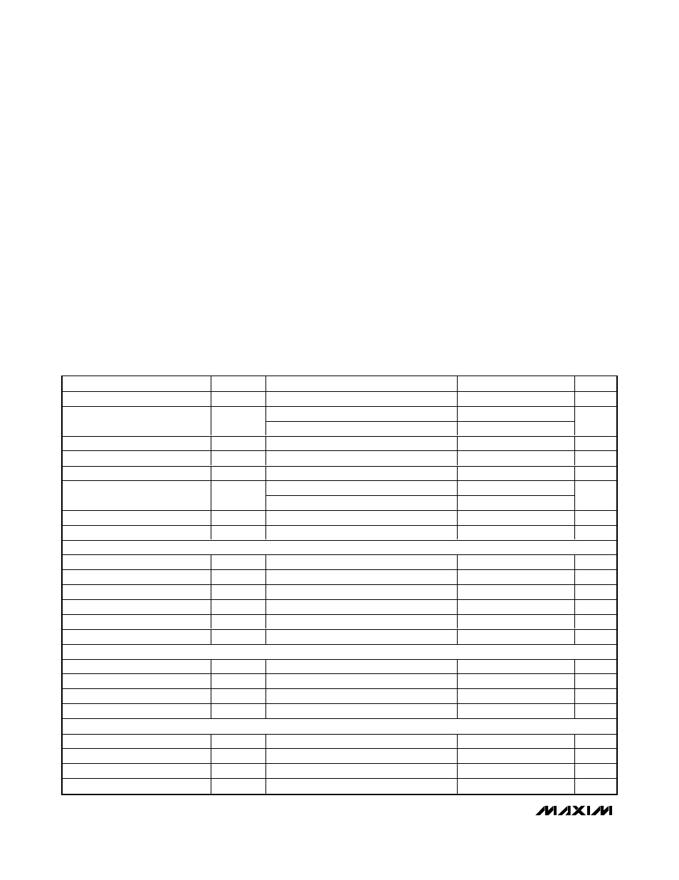
ELECTRICAL CHARACTERISTICS
(V
IN
= 12V, C
REG
= 0.1µF, I
REG
= 0, C
LGC
= 15nF, V
DIM1
= V
DIM2
= V
DIM3
= 3.4V, R
CS_
= 2.85Ω from CS_ to GND, T
J
= T
A
= -40°C
to +125°C, unless otherwise noted. Typical values are at T
A
= +25°C.) (Note 1)
Stresses beyond those listed under “Absolute Maximum Ratings” may cause permanent damage to the device. These are stress ratings only, and functional
operation of the device at these or any other conditions beyond those indicated in the operational sections of the specifications is not implied. Exposure to
absolute maximum rating conditions for extended periods may affect device reliability.
PARAMETER
SYMBOL
CONDITIONS
MIN
TYP
MAX
UNITS
Supply Voltage Range
V
IN
5.5
40
V
V
IN
rising
4.4
4.9
5.4
Undervoltage Lockout
UVLO
V
IN
falling
4.0
4.6
5.2
V
Ground Current
I
G
I
OUT1
= I
OUT2
= I
OUT3
= 70mA
1.5
3
mA
Guaranteed Output Current
I
OUT
70
mA
LED Current-Sense Accuracy
5mA ≤ I
OUT_
≤ 70mA
5
%
I
OUT_
= 70mA, 6.5V ≤ V
IN
≤ 40V
0.3
0.7
Dropout Voltage (Note 2)
∆VDO
I
OUT_
= 70mA, 5.5V ≤ V
IN
≤ 6.5V
0.3
0.8
V
Output Current Slew Rate
8
mA/µs
Short-Circuit Current
V
OUT_
= 0V
180
mA
LEDGOOD
LEDGOOD Output Logic Low
V
OL
I
SINK
= 2mA
0.4
V
LGC Pullup Resistor
65
100
135
kΩ
LGC Input Upper Threshold
V
UTH
2.53
V
LGC Input Lower Threshold
V
LTH
0.8
V
LGC Pulldown Current
V
LGC
> V
UTH
20
mA
LGC Clock Period
C
LGC
= 15nF
0.77
1.5
2.3
ms
DIMMING INPUT (DIM1, DIM2, DIM3)
DIM_ Logic-Input Bias Current
I
DIM_
-0.1
+0.1
µA
DIM_ Input-Voltage High
2.4
V
IN
V
DIM_ Input-Voltage Low
0.6
V
DIM_ Frequency
0
3
kHz
OUTPUTS (OUT1, OUT2, AND OUT3) (Note 3)
Turn-On Time
DIM_ rising edge to 90% of OUT_ current
12
28
µs
Turn-Off Time
DIM_ falling edge to 10% of OUT_ current
8
18
µs
Output Current Rise Time
10% to 90%
7
18
µs
Output Current Fall Time
90% to 10%
6
15
µs
IN to GND ...............................................................-0.3V to +45V
OUT1, OUT2, OUT3, DIM1, DIM2,
DIM3 to GND ...........................................-0.3V to (V
IN
+ 0.3V)
REG, LGC, LEDGOOD to GND ................................-0.3V to +6V
CS1, CS2, CS3 to GND .........................................-0.3V to +0.5V
OUT1, OUT2, OUT3 Short Circuited
to GND Duration (V
IN
+ 16V) ..........................................60min
Maximum Current into Any Pin
(except IN, OUT1, OUT2, OUT3)..................................±20mA
Continuous Power Dissipation (T
A
= +70°C)
16-Pin TQFN 5mm x 5mm
(derate 33.3mW/°C above +70°C) .........................2666mW
16-Pin TSSOP (derate 26.1mW/°C above +70°C) ....2088.8mW
Operating Temperature Range .........................-40°C to +125°C
Junction Temperature ......................................................+150°C
Storage Temperature Range .............................-65°C to +150°C
Lead Temperature (soldering, 10s) .................................+300°C