Chip information – Rainbow Electronics MAX5123 User Manual
Page 18
MAX5122/MAX5123
+5V/+3V, 12-Bit, Serial, Force/Sense DACs
with 10ppm/°C Internal Reference
18
______________________________________________________________________________________
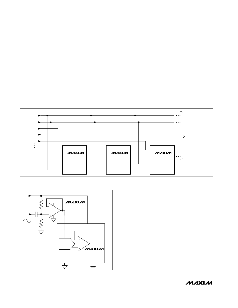
Using an External Reference
with AC Components
The MAX5122/MAX5123 have multiplying capabilities
within the reference input voltage range specifications.
Figure 13 shows a technique for applying a sinusoidal
input to REF, where the AC signal is offset before being
applied to the reference input.
Power-Supply and Bypassing
Considerations
On power-up, the input and DAC registers are cleared to
either zero (RSTVAL = DGND) or midscale (RSTVAL =
V
DD
). Bypass the power supply (V
DD
) with a 4.7µF
capacitor in parallel with a 0.1µF capacitor to AGND.
Minimize lead lengths to reduce lead inductance.
Layout Considerations
Digital and AC signals coupling to AGND can create
noise at the output. Connect AGND to the highest quali-
ty ground available. Use proper grounding techniques,
such as a multilayer board with a low-inductance
ground plane. Wire-wrapped boards and sockets are
not recommended. If noise becomes an issue, shield-
ing may be required.
TO OTHER
SERIAL DEVICES
MAX5122
MAX5123
DIN
SCLK
CS
MAX5122
MAX5123
DIN
SCLK
CS
MAX5122
MAX5123
DIN
I
II
III
SCLK
CS
DIN
SCLK
CS1
CS2
CS3
Figure 12. Multiple Devices Share One Common Digital Input (DIN)
DAC
OUT
MAX5122
MAX5123
10k
26k
REF
FB
V
DD
DGND
AGND
+5V/
+3V
AC
REFERENCE
INPUT
500mVp-p
MAX495
+5V/+3V
___________________Chip Information
TRANSISTOR COUNT: 3308
SUBSTRATE CONNECTED TO AGND
Figure 13. External Reference with AC Components