Table 3. detailed sspcon register contents, Table 4. detailed sspstat register contents – Rainbow Electronics MAX5123 User Manual
Page 14
MAX5122/MAX5123
+5V/+3V, 12-Bit, Serial, Force/Sense DACs
with 10ppm/°C Internal Reference
14
______________________________________________________________________________________
Serial Data Output
The contents of the internal shift-register are output
serially on DOUT which allows for daisy-chaining of
multiple devices (see
Applications Information
) as well
as data readback. The MAX5122/MAX5123 may be
programmed to shift data out of DOUT on the serial
clock’s rising edge (Mode 1) or on the falling edge
(Mode 0). The latter is the default during power-up and
provides a lag of 16 clock cycles, maintaining SPI,
QSPI, MICROWIRE, and PIC16/PIC17 compatibility. In
Mode 1, the output data lags DIN by 15.5 clock cycles.
During power-down, DOUT retains its last digital state
prior to shutdown.
User-Programmable Output (UPO)
The UPO feature allows an external device to be con-
trolled through the serial-interface setup (Table 1) there-
by reducing the number of microcontroller I/O ports
required. During power-down, this output will retain the
last digital state before shutdown. With CLR pulled low,
UPO will reset to the default state after wake-up.
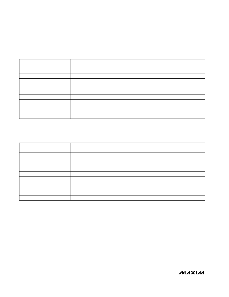
Table 3. Detailed SSPCON Register Contents
Receive Overflow Detect Bit
X
SSPOV
BIT6
BIT7
Clock Polarity Select Bit. CKP = 0 for SPI master-mode selection.
0
CKP
BIT4
BIT5
Synchronous Serial Port Enable Bit.
0: Disables serial port and configures these pins as I/O port pins.
1: Enables serial port and configures SCK, SDO and SCI as serial-
port pins.
1
SSPEN
0
SSPM2
BIT2
BIT3
1
SSPM0
BIT0
BIT1
CONTROL BIT
0
SSPM1
Write Collision Detection Bit
X
WCOL
SYNCHRONOUS SERIAL-PORT CONTROL REGISTER
(SSPCON)
MAX5122/MAX5123
SETTINGS
Synchronous Serial Port Mode Select Bit. Sets SPI master mode
and selects f
CLK
= f
OSC
/ 16
0
SSPM3
X = Don’t care
Table 4. Detailed SSPSTAT Register Contents
X = Don’t care
SPI Clock Edge Select Bit. Data will be transmitted on the rising
edge of the serial clock.
1
CKE
BIT6
Buffer Full Status Bit
BIT7
Update Address
Read/Write Bit Information
Stop Bit
X
P
BIT4
BIT5
Data Address Bit
X
D/A
X
R/W
BIT2
BIT3
X
BF
BIT0
BIT1
CONTROL BIT
X
UA
SPI Data Input Sample Phase. Input data is sampled at the mid-
dle of the data output time.
0
SMP
SYNCHRONOUS SERIAL-PORT CONTROL REGISTER
(SSPSTAT)
MAX5130/MAX5131
SETTINGS
Start Bit
X
S